ave up to 70% on SMT Parts – In Stock & Ready to Ship

Get Quote →

Wire Bonder Machine & ASM Wire Bonding Technology Platform

Wire bonder machines are core semiconductor packaging systems used to connect integrated circuits using ultra-fine wire bonding technology. ASM wire bonder systems support advanced packaging, automotive chips, and high-density IC manufacturing.

What is a Wire Bonder Machine?

Definition

A wire bonder machine is a semiconductor packaging system used to electrically connect integrated circuits (ICs) to substrates or lead frames using ultra-fine bonding wires such as gold, copper, or aluminum.

ASM wire bonder platforms are widely used in advanced semiconductor manufacturing, automotive electronics, and high-density chip packaging due to their precision, stability, and high-speed bonding capability.
ASM Wire Bonder Machine

Wire Bonding Physics & Process Mechanism

Ultrasonic Energy
High-frequency vibration breaks oxide layer and enables atomic bonding.
Thermosonic Bonding
Combination of heat + pressure + ultrasonic energy.
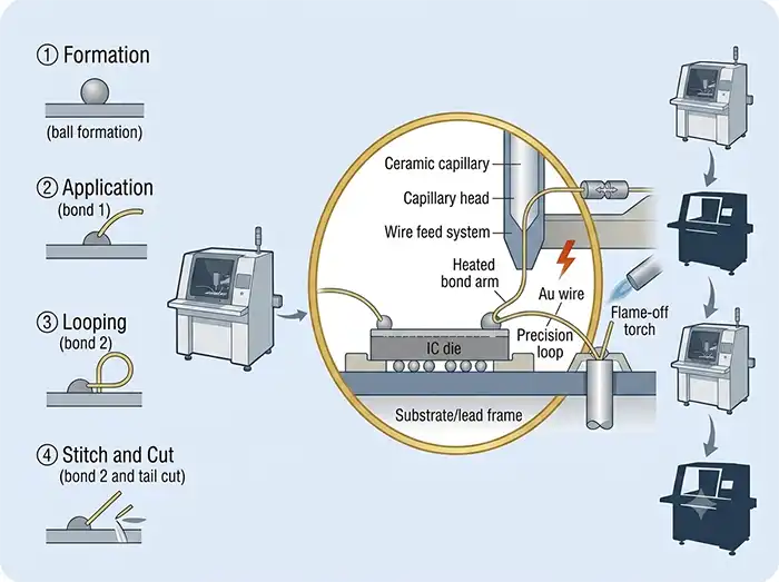
Ball Formation (EFO)
Electric flame-off creates free air ball for first bond.
Loop Formation
Controlled wire geometry ensures mechanical stability.
Second Bond
Wire attaches to substrate or lead frame.
Cut & Reset
Wire is cut and system resets for next cycle.

Wire Bonder Machine Architecture

Bond Head System
Controls ultrasonic energy, capillary movement, and bonding force.
Vision System
High-resolution alignment for micro-scale precision bonding.
Motion System
X-Y-Z stage ensures micron-level positioning accuracy.
Control System
Real-time process control for temperature, force, and loop shape.

Wire Bonder Machine Types

Type Description Application
Fully Automatic High-speed production line system Mass semiconductor packaging
Semi-Automatic Operator-assisted system R&D & small batch production
Heavy Wire Bonder Thick wire bonding system Power semiconductor devices
Fine Wire Bonder Ultra-precision micro bonding Advanced IC packaging

ASM Wire Bonder Technology Position in Semiconductor Industry

ASM is widely recognized as a key technology provider in advanced semiconductor packaging equipment, particularly in high-precision wire bonding systems used in IC assembly and backend manufacturing processes.

Its wire bonder platforms are engineered to deliver high-speed, high-accuracy interconnection between silicon chips and substrate materials, supporting critical requirements in automotive electronics, high-performance computing (HPC), and advanced packaging applications.

Unlike conventional bonding systems, ASM wire bonder solutions integrate multi-axis motion control, real-time vision alignment, and adaptive bonding force control, enabling stable production in ultra-fine pitch environments.

ASM AERO wire bonder represents the next generation of ASM bonding architecture, designed for advanced packaging nodes such as 2.5D integration, high-density interconnect (HDI), and next-generation semiconductor devices.

Key technology advantages include:
- Ultra-high precision motion control at micron-level accuracy
- Advanced vision system for automatic alignment correction
- Stable thermosonic bonding for fine wire applications
- High throughput capability for mass production environments
- Process stability for automotive-grade reliability standards

Wire Bonder Machine Comparison

Feature ASM K&S BESI
Precision Ultra High High High
Speed High Medium Medium
Advanced Packaging Strong Medium Strong
Automation High Medium High

Industrial Applications of Wire Bonder Machines

Semiconductor IC Packaging
Wire bonder machines are widely used in integrated circuit packaging to establish electrical interconnections between chip pads and substrate layers using ultra-fine bonding wires. This is a core process in modern semiconductor backend manufacturing.
Automotive Power Devices
Used in power semiconductor modules such as IGBT, MOSFET, and SiC devices, where high thermal stability and long-term reliability are critical under harsh automotive environments.
Memory & Storage Devices
Applied in DRAM, NAND flash, and advanced memory packaging, requiring high-density interconnect and consistent bonding accuracy at micro-scale pitch levels.
LED & Optoelectronics
Supports LED chip packaging and optoelectronic device assembly, ensuring stable electrical connection and light efficiency performance in high-volume production.
Advanced Packaging (2.5D / 3D)
Critical for heterogeneous integration technologies, including chip stacking, interposer-based packaging, and high-bandwidth computing systems.
RF & High-Frequency Devices
Used in RF modules, communication chips, and high-frequency semiconductor devices where signal integrity and low parasitic effects are essential.

Wire Bonder vs Die Bonder vs Flip Chip Bonder

In semiconductor backend manufacturing, different bonding technologies are used depending on packaging structure, electrical performance requirements, and production cost targets. Understanding the differences between these systems is critical when selecting the right equipment for a production line.

Category Wire Bonder Die Bonder Flip Chip Bonder
Core Function Connects chip pads to substrate using fine bonding wire Places and attaches die onto substrate or lead frame Directly attaches flipped chip using solder bumps or copper pillars
Interconnect Method Wire bonding (Au / Cu / Al wire) Adhesive or epoxy die attach Bump-based direct connection
Process Complexity Moderate, highly optimized mature process Low to moderate depending on automation level High, requires precise alignment and advanced process control
Precision Requirement Micron-level bonding accuracy Moderate placement accuracy Ultra-high precision for fine pitch interconnects
Typical Applications IC packaging, LED, automotive electronics Chip placement in module assembly High-performance computing, advanced packaging, 2.5D/3D integration
Technology Maturity Highly mature and widely used Mature and cost-efficient Advanced and rapidly evolving
Cost Level Medium Low to medium High

Key Insight:
Wire bonding remains the most widely adopted interconnection method in semiconductor manufacturing due to its balance of cost, reliability, and process maturity. However, flip chip and die bonding technologies are increasingly used in advanced packaging environments where performance density is critical.

In most production environments, these technologies are not mutually exclusive but coexist at different packaging stages and product categories.

ASM AERO Wire Bonder vs Standard Wire Bonder

In advanced semiconductor packaging, not all wire bonding systems deliver the same level of precision, speed, and process stability. ASM AERO represents a next-generation platform designed for high-density and advanced packaging applications, while standard wire bonders are typically used for general IC assembly.

Feature ASM AERO Wire Bonder Standard Wire Bonder
Target Application Advanced packaging (2.5D / 3D IC, HPC, automotive-grade chips) General IC packaging and standard semiconductor devices
Precision Level Ultra-high precision with advanced alignment correction Standard micron-level accuracy
Motion Control System Advanced multi-axis adaptive motion system Conventional motion control architecture
Vision System High-resolution real-time adaptive vision alignment Standard vision alignment system
Process Stability Optimized for ultra-fine pitch and complex substrates Stable for conventional packaging processes
Throughput Capability High-speed optimized for advanced production lines Moderate to high depending on configuration
Typical Usage Advanced semiconductor fabs and OSATs Mainstream semiconductor packaging facilities

Key Insight:
ASM AERO systems are specifically engineered for next-generation semiconductor packaging where precision density, signal integrity, and process stability are critical. Standard wire bonders remain widely used for cost-efficient, high-volume production environments.

Maintenance & Failure Factors in Wire Bonder Operation

In long-term semiconductor production environments, wire bonder machines operate under high-speed, high-frequency mechanical cycling. Over time, certain components naturally degrade and may affect bonding stability, yield rate, and process consistency.

Common issues observed in production environments include:

- Bond head wear leading to unstable bonding force or inconsistent loop formation - Capillary contamination caused by residue buildup or improper cleaning cycles - Vision system misalignment resulting in inaccurate pad positioning during bonding - Wire feed instability caused by friction variation or spool tension imbalance - Thermal drift affecting bonding energy consistency in continuous production

These issues typically do not appear suddenly, but gradually impact process stability, leading to subtle yield fluctuation before visible failure occurs.

Regular preventive maintenance is usually required in the following areas:
- Bond head calibration and wear inspection - Capillary replacement scheduling based on cycle count - Vision system alignment verification - Wire feed path cleaning and tension adjustment - Temperature stability monitoring in bonding environment

In high-volume semiconductor manufacturing, maintaining stable bonding quality is often more dependent on preventive maintenance strategy than on machine performance alone.

How to Select a Wire Bonder Machine for Production Requirements

Selecting a wire bonder is not only a specification comparison process, but also a decision based on production stability, device compatibility, and long-term manufacturing cost control.

In actual semiconductor production planning, the following factors are typically evaluated:

1. Bonding speed and throughput requirement
Production lines with high-volume IC output require stable high-speed bonding capability without sacrificing positional accuracy or loop consistency.

2. Wire material compatibility
Different applications require gold (Au), copper (Cu), or aluminum (Al) wire. Material selection directly affects bonding temperature, force control, and long-term reliability.

3. Precision and process window stability
Advanced packaging requires micron-level alignment accuracy. A stable process window is often more important than peak machine specification.

4. Automation level and production environment
Fully automated systems are preferred in mass production environments, while semi-automatic systems are typically used in R&D or low-volume production.

5. Application scenario and device type
Requirements vary significantly between standard IC packaging, automotive power devices, and advanced packaging structures such as 2.5D/3D integration.

6. Lifecycle cost consideration
Beyond initial machine investment, maintenance cost, consumable parts availability, and downtime risk must also be considered in total cost of ownership (TCO).

In practice, many manufacturers choose equipment not only based on specifications, but based on long-term production stability and service support capability.

Why do so many people choose to work with GeekValue?

Our brand is spreading from city to city, and countless people have asked me, "What is GeekValue?" It stems from a simple vision: to empower Chinese innovation with cutting-edge technology. This is a brand spirit of continuous improvement, hidden in our relentless pursuit of detail and the delight of exceeding expectations with every delivery. This almost obsessive craftsmanship and dedication is not only the persistence of our founders, but also the essence and warmth of our brand. We hope you will start here and give us an opportunity to create perfection. Let us work together to create the next "zero defect" miracle.

Details

Contact a sales expert

Reach out to our sales team to explore customized solutions that perfectly meet your business needs and address any questions you may have.

Sales Request

Follow Us

Stay connected with us to discover the latest innovations, exclusive offers, and insights that will elevate your business to the next level.

kfweixin

Scan to add WeChat

Request Quote