ave up to 70% on SMT Parts – In Stock & Ready to Ship
Get Quote →Reliable electroplating equipment for wafer bumping, redistribution layers, copper plating, nickel plating, gold plating, MEMS, compound semiconductor, and advanced packaging production.
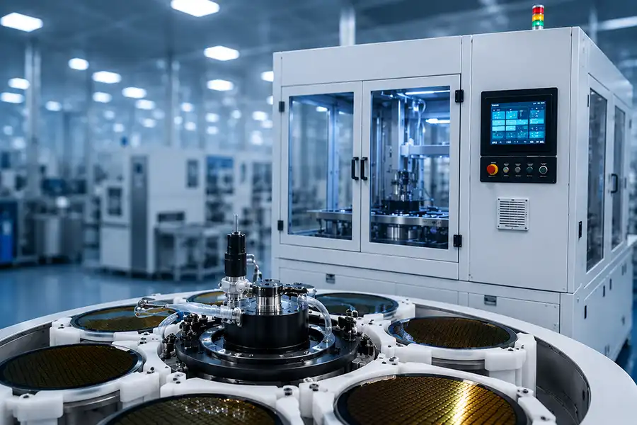
This equipment is built for controlled wet processing where metal thickness, adhesion, surface quality, and process repeatability are important to final production results.
The system deposits metal layers onto wafers, substrates, or microstructures through electrochemical plating. It supports processes where controlled thickness, clean surface condition, and stable deposition are required.
Plating quality depends on bath chemistry, filtration, temperature, current distribution, wafer contact, and handling safety. A suitable system helps maintain stable process conditions during production.
We provide available equipment options based on your wafer size, plating metal, process application, production capacity, delivery timeline, and preferred machine condition.
Explore available equipment for wafer-level packaging, copper plating, nickel plating, gold plating, MEMS, compound semiconductor, and advanced packaging applications.
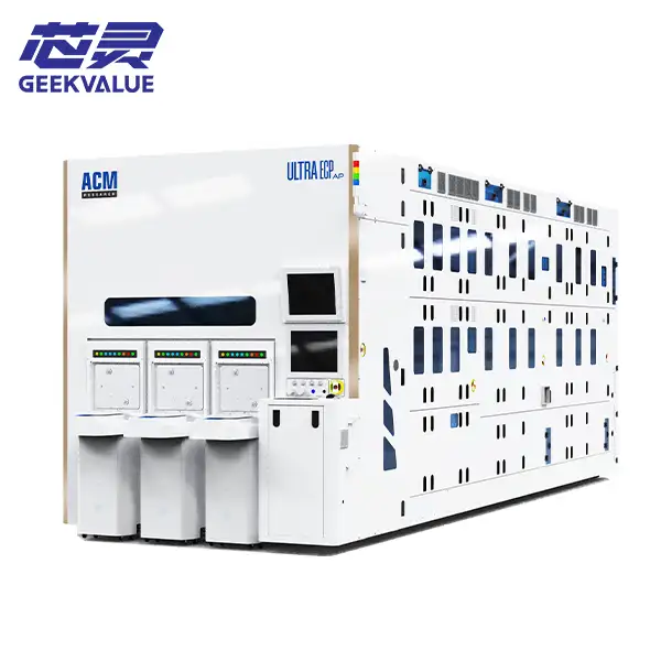
ACM Research’s ULTRA ECP ap-p is a groundbreaking panel-level horizontal plating system.
Check Stock & Quote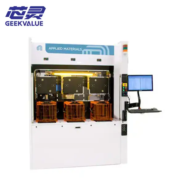
Applied Materials' Raider® Edge ECD system is an electrochemical deposition (ECD) device used in semiconductor manu...
Check Stock & Quote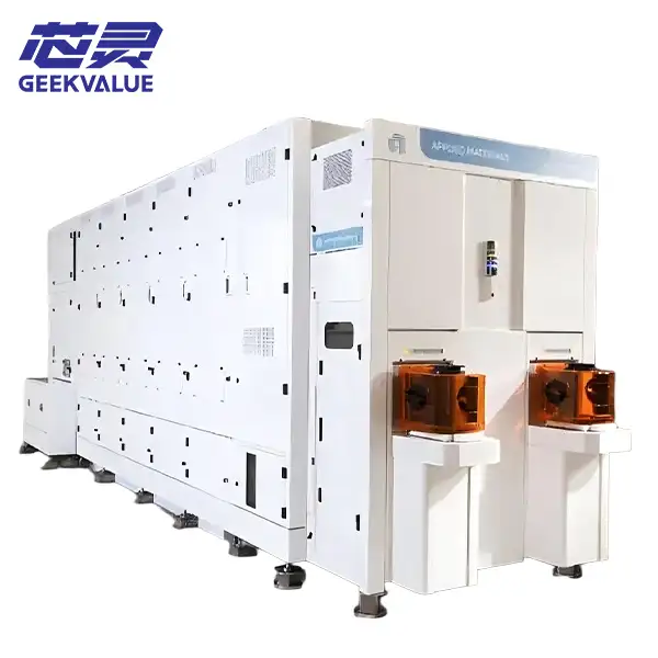
Applied Materials' Nokota™ ECD is a high-productivity electrochemical deposition system designed specifically for w...
Check Stock & QuoteIn wafer-level production, electroplating quality directly affects downstream packaging, electrical performance, inspection results, and production yield.
A reliable system helps reduce unstable plating results and supports cleaner, more repeatable production.
The process combines wafer preparation, controlled bath conditions, electrical deposition, rinsing, drying, and inspection readiness.
The wafer is cleaned, patterned, seeded, and prepared before entering the plating step.
The wafer is loaded into a process cell with suitable clamping, contact, and handling design.
Chemistry, circulation, filtration, additives, and temperature are controlled for process stability.
Electrical current drives metal ion deposition according to the required recipe and process target.
After plating, wafers are rinsed, dried, and prepared for inspection or the next production step.
Semiconductor electroplating systems are used in multiple wafer-level and packaging-related production processes.
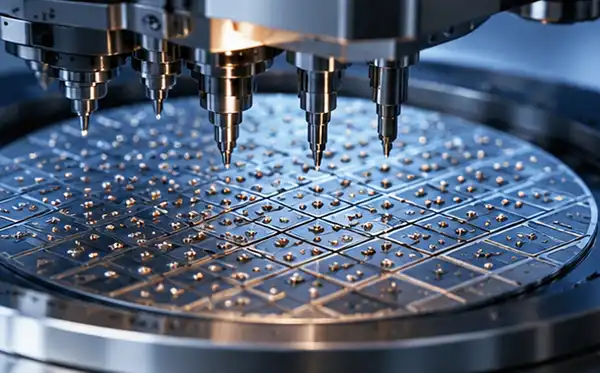
Used to form solder bumps, copper pillars, nickel barriers, and related bump structures for flip chip and wafer-level packaging.
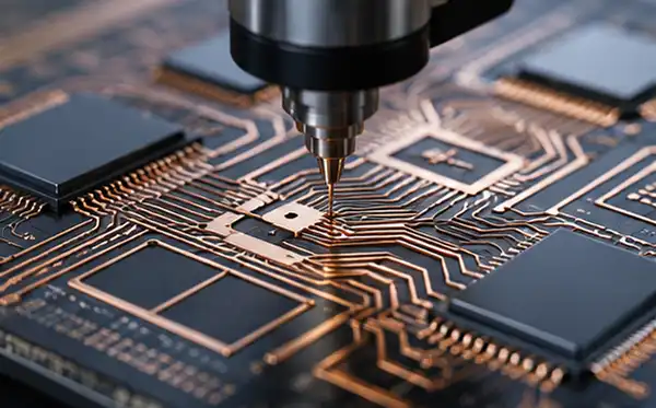
Supports copper redistribution layer processes for fan-out packaging, wafer-level routing, and high-density interconnect structures.
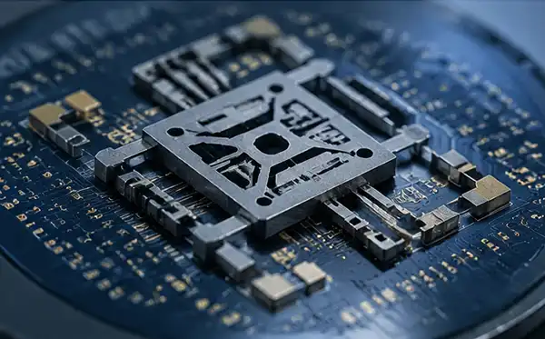
Used to build metal microstructures, sensor features, contact layers, actuators, and other functional structures for MEMS devices.
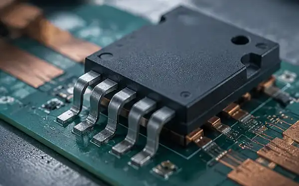
Supports metallization and packaging-related plating processes for GaN, GaAs, SiC, and power semiconductor devices.
A semiconductor electroplating system should support controlled deposition quality, safe wafer handling, and stable wet process conditions.
Helps maintain consistent deposition across wafer surfaces and patterned areas.
Stable current control supports repeatable plating for different wafer patterns and metal layers.
Filtration and circulation help reduce particles, pits, nodules, and rough plating surfaces.
Bath temperature control helps maintain plating rate, additive behavior, and process consistency.
Proper loading, clamping, and transfer help reduce wafer damage and contamination risk.
Supports different plating metals, wafer sizes, production needs, and automation levels.
Better equipment control helps improve plating consistency and supports smoother downstream production.
Purchasing semiconductor equipment requires more than a quotation. You need suitable machine selection, clear communication, equipment condition checks, delivery support, and practical sourcing efficiency.
We help customers find suitable equipment based on real production needs, budget, and timeline.
Check Stock & QuoteWe help check available new, used, and refurbished semiconductor electroplating systems according to your project needs.
We match equipment according to wafer size, plating metal, thickness target, production capacity, and process application.
Available machines can be checked before shipment to help reduce purchasing risk.
We respond quickly to machine inquiries and help you check suitable equipment options efficiently.
We support packing, export documentation, and international shipment for overseas buyers.
Related wafer processing, packaging, bonding, inspection, and wet process equipment can also be sourced together.
The right electroplating system depends on your wafer size, plating metal, process purpose, uniformity target, chemical requirements, automation level, and production capacity.
Send us your process details, and we will help check suitable equipment options.
Check Stock & QuoteIt is wet process equipment used to deposit controlled metal layers onto wafers, substrates, or microstructures through electrochemical plating.
It can be used for wafer bumping, redistribution layers, copper plating, nickel plating, gold plating, MEMS, compound semiconductor devices, and advanced packaging.
Common plating metals include copper, nickel, gold, tin, solder materials, and other specialty metals depending on process requirements.
Please provide wafer size, plating metal, target thickness, process application, required capacity, preferred machine condition, and facility requirements if available.
Yes. We can help check available new, used, and refurbished equipment options based on your budget and project timeline.
Yes. We can help review basic requirements such as wafer size, metal type, application, automation level, and equipment condition before recommending options.
Yes. We support packing, export documentation, and international shipping for overseas equipment buyers.
The price depends on system configuration, wafer size, process capability, automation level, machine condition, brand, and availability.
Why do so many people choose to work with GeekValue?
Our brand is spreading from city to city, and countless people have asked me, "What is GeekValue?" It stems from a simple vision: to empower Chinese innovation with cutting-edge technology. This is a brand spirit of continuous improvement, hidden in our relentless pursuit of detail and the delight of exceeding expectations with every delivery. This almost obsessive craftsmanship and dedication is not only the persistence of our founders, but also the essence and warmth of our brand. We hope you will start here and give us an opportunity to create perfection. Let us work together to create the next "zero defect" miracle.
DetailsContact a sales expert
Reach out to our sales team to explore customized solutions that perfectly meet your business needs and address any questions you may have.

© All Rights Reserved. Technical Support:TiaoQingCMS
 EN
EN id
id sk
sk sr
sr sv
sv it
it pt
pt bn
bn ms
ms be
be nl
nl fr
fr th
th vi
vi ru
ru ja
ja ko
ko de
de hy
hy az
az bs
bs bg
bg my
my cs
cs da
da dv
dv el
el et
et fil
fil fi
fi ga
ga gl
gl gn
gn he
he hi
hi km
km hr
hr hu
hu is
is kn
kn rw
rw lo
lo lv
lv lt
lt lb
lb lg
lg mi
mi mt
mt ne
ne no
no ny
ny or
or om
om per
per pl
pl ro
ro sa
sa so
so es
es sw
sw ta
ta tr
tr uk
uk ur
ur cy
cy xh
xh