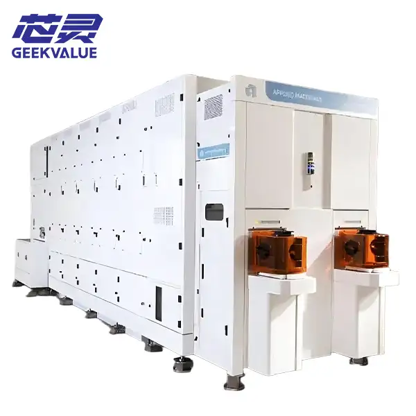
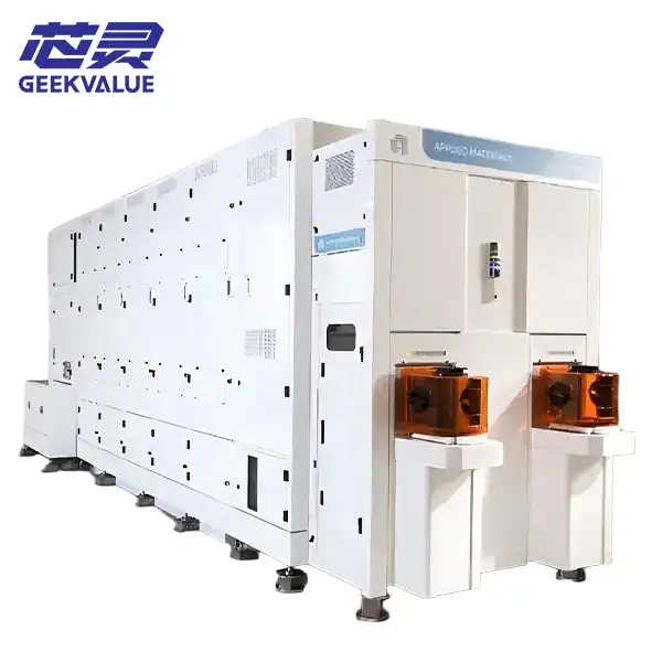
 Applied Materials’ Nokota™ ECD is a high-productivity electrochemical deposition system designed specifically for advanced wafer-level packaging.
**The System’s Core: More Than Just Electroplating—A Comprehensive Process Platform**
The Nokota system is not merely an electroplating tool; it offers a comprehensive suite of solutions tailored to address the specific challenges inherent in advanced packaging workflows. Its core technical features include:
**Broad Metal and Wafer Support:** Supports the deposition of a wide range of metals—including copper, tin-silver alloys, nickel, gold, tin, and palladium—and is compatible with 150mm, 200mm, and 300mm wafers.
**Flexible System Scalability:** Features a unique single-chamber configurability design, departing from traditional paired-chamber architectures. The system scales seamlessly from R&D and pilot runs to high-volume manufacturing, and can be rapidly reconfigured within a single day—making it ideally suited for production environments that require agile responsiveness to market shifts.
**Three Core Advantages**
According to Applied Materials’ official positioning, the Nokota system’s core competitive advantages are concentrated in the following three areas:
**Unrivaled Wafer Protection Capabilities: SafeSeal™ and HotSwap™**
In packaging processes, protecting the wafer from particulate contamination is paramount. The Nokota system addresses this critical pain point through two innovative technologies:
**SafeSeal™ Technology:** An industry-first, fully automated wafer protection technology. By performing vacuum integrity checks on the wafer prior to processing—and maintaining protection throughout the entire single- or multi-metal plating sequence—it enables a "single-seal" workflow, effectively mitigating the risk of damage associated with repeated sealing and unsealing cycles.
**HotSwap™ Technology:** Allows for the automated replacement of sealing components without interrupting production, thereby fundamentally eliminating equipment downtime caused by seal maintenance requirements.
**Industry-Leading Productivity**
**Cost-Effectiveness and Availability:** The aforementioned combination of technologies enables the Nokota system to deliver an additional 330 hours of production time annually, while simultaneously reducing wafer scrap rates through enhanced wafer protection capabilities.
**High-Performance Process Chambers (VMax™):** The VMax™ process chambers feature optimized mass transport, enabling higher plating rates and superior coplanarity. Furthermore, each chamber integrates an in-situ cleaning function to minimize particulate contamination.
**Rapid and Flexible Configuration Capabilities**
This represents another major advantage conferred by the system’s modular design. It not only supports seamless switching between the aforementioned various wafer sizes but also enables rapid transitions between different packaging methods (such as bumping, RDL, TSV, etc.)—a capability that is crucial in today's landscape of diversified packaging types.
Key Specifications and Application Scenarios
Technical Specifications at a Glance
Equipment Type: High-Productivity Wafer-Level Packaging Electrochemical Deposition System
Supported Wafer Sizes: 150mm, 200mm, 300mm; supports simultaneous processing of two different sizes within the same system
Supported Metals: Copper (Cu), Tin-Silver (SnAg), Nickel (Ni), Gold (Au), Palladium (Pd), etc.
Process Applications: Bumping (Pillar/Bump), Redistribution Layer (RDL), Through-Silicon Via (TSV) Filling
Key Features: SafeSeal™ Fully Automated Wafer Protection, HotSwap™ Seal Ring Hot-Swapping, VMax™ High-Performance Chamber
Availability/Productivity: Delivers over 330 additional production hours per year; offers the industry's lowest cost of ownership
Target Application Areas
Advanced Packaging: Pillars/Bumps, Redistribution Layers (RDL), and Through-Silicon Vias (TSV)
Packaging Technologies: 2.5D/3D Packaging, Fan-Out Packaging, Wafer-Level Chip-Scale Packaging (WLCSP), etc.
Emerging Applications: Providing packaging support for IoT devices, sensors, 5G communication systems, power devices, and more.
High-Performance Computing: Plays a pivotal role in the fabrication of micro-bumps for High Bandwidth Memory (HBM).
Summary
The Nokota™ ECD system precisely addresses the urgent demands of advanced packaging for high yield, high flexibility, and high productivity. Through technologies such as SafeSeal™ and HotSwap™, it resolves the reliability pain points inherent in traditional processes; furthermore, leveraging its flexible modular platform, it provides chip manufacturers with a solution that delivers both cost and efficiency advantages within a complex and ever-changing market landscape.