ave up to 70% on SMT Parts – In Stock & Ready to Ship
Get Quote →Permanent high-contrast marking for wafers, semiconductor packages, modules, and electronic devices. Built for traceability, code readability, automated production, and reliable device identification.
Laser marking helps manufacturers create durable and readable marks on wafers, packages, modules, and components for traceability and production control.
Mark wafers, packages, or devices with Data Matrix codes, QR codes, serial numbers, batch numbers, logos, and custom identification formats.
Laser marking creates clean and readable marks that support inspection, sorting, production tracking, and downstream identification.
The system can be used in standalone or inline production environments and can support automated loading, code generation, and data communication.
Explore available equipment for wafer marking, package marking, Data Matrix coding, traceability, and semiconductor production line identification.
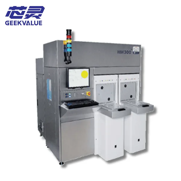
The ThinkLaser HM300 is a specialized, industrial-grade device fundamentally designed to provide permanent wafer marking...
Check Stock & Quote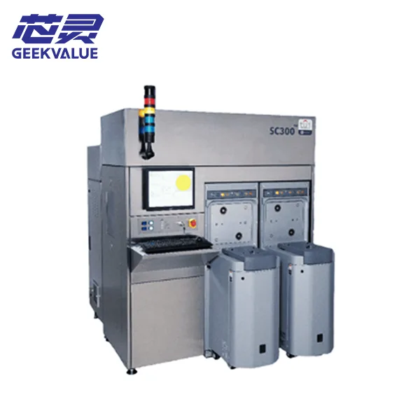
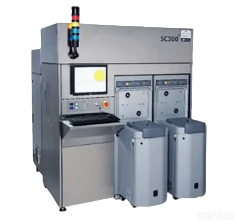
The ThinkLaser SC300 is a high-end, fully automated "Soft Marking" laser marking system designed specifically ...
Check Stock & Quote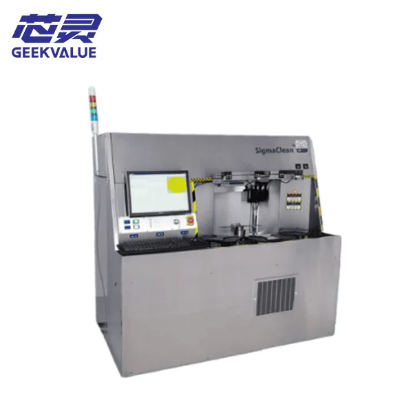
ThinkLaser SigmaClean is a fully automated soft-marking laser marking system designed specifically for 100mm to 200mm wa...
Check Stock & Quote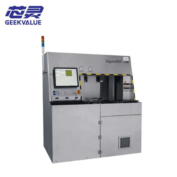
The core positioning of ThinkLaser SigmaDSC is that of a fully automated "Hard Marking" laser marking system—s...
Check Stock & QuoteLaser marking supports reliable product identification without labels, ink, or contact-based marking. It is suitable for high-volume semiconductor production where readability and traceability are important.
Track each wafer, package, module, or device through production, testing, packaging, shipment, and after-sales quality control.
Marks remain readable during handling, testing, packaging, and long-term product use.
Supports automatic code generation, machine vision inspection, inline loading, and data communication with production systems.
Suitable for mass production of semiconductor packages, electronic modules, and precision components.
The machine can be configured for different marking objects in semiconductor and electronics manufacturing.
Wafer ID, batch code, tracking code, and process identification.
Package marking for BGA, QFN, QFP, SOP, CSP, and related devices.
Laser marking for power modules, sensors, MEMS modules, and assemblies.
Final identification, production tracking, and shipping traceability.
Suitable configurations can be selected according to package material, size, surface finish, and marking requirement.
Different materials require different laser sources. Choosing the right laser helps improve contrast, reduce thermal effect, and protect device quality.
| Laser Technology | Best For | Typical Use |
|---|---|---|
| Fiber Laser | Metal surfaces and some package materials | Package codes, metal components, serial numbers, and durable identification. |
| UV Laser | Sensitive materials and fine marking | High-contrast marking with lower thermal impact on delicate devices. |
| Green Laser | Precision marking and special materials | Fine feature marking where controlled energy absorption is required. |
| CO₂ Laser | Plastic and organic package materials | Marking on suitable plastic package surfaces and non-metal materials. |
The machine can be integrated into semiconductor packaging and testing workflows to support continuous identification and quality tracking.
Laser marking helps replace unstable manual or label-based identification with durable, automated, and readable marking.
We help customers source suitable semiconductor laser marking machines based on package type, marking format, material sensitivity, throughput, and production integration needs.
Our support is focused on practical machine matching, fast availability checking, and one-stop semiconductor equipment sourcing.
Flexible supply of available machines, used systems, and refurbished equipment according to your budget.
Recommend suitable configurations according to package material, code type, marking area, and throughput.
Laser marking can be sourced together with die bonders, wire bonders, plasma cleaners, AOI, and test handlers.
Support for equipment packing, export documentation, and international shipment.
The right machine depends on device material, package type, marking content, code size, contrast requirement, cycle time, automation level, and production line integration.
Send us your package type, marking sample, code format, and production capacity. We will help check suitable available equipment.
It is a marking system used to create permanent identification on wafers, semiconductor packages, modules, and electronic devices.
Common formats include Data Matrix codes, QR codes, barcodes, serial numbers, batch numbers, logos, and custom characters.
Yes. Semiconductor laser marking machines are commonly used for small, high-contrast Data Matrix codes that support traceability.
With the correct laser source, power, speed, focus, and process settings, marking can be controlled to reduce thermal impact and protect the device surface.
Common package types include BGA, QFN, QFP, SOP, TSOP, CSP, MEMS, power devices, wafers, modules, and related semiconductor components.
Fiber laser is often used for metal or durable marking applications, while UV laser is suitable for sensitive materials and fine marking with lower thermal influence.
Many systems can support data communication, automatic code generation, vision alignment, and production line integration depending on configuration.
You should consider package type, material surface, code format, marking contrast, throughput, loading method, automation level, and integration requirements.
Send us your package type, marking format, material surface, code size, and production capacity. We will help you check suitable available equipment options.
Why do so many people choose to work with GeekValue?
Our brand is spreading from city to city, and countless people have asked me, "What is GeekValue?" It stems from a simple vision: to empower Chinese innovation with cutting-edge technology. This is a brand spirit of continuous improvement, hidden in our relentless pursuit of detail and the delight of exceeding expectations with every delivery. This almost obsessive craftsmanship and dedication is not only the persistence of our founders, but also the essence and warmth of our brand. We hope you will start here and give us an opportunity to create perfection. Let us work together to create the next "zero defect" miracle.
DetailsContact a sales expert
Reach out to our sales team to explore customized solutions that perfectly meet your business needs and address any questions you may have.

© All Rights Reserved. Technical Support:TiaoQingCMS
 EN
EN id
id sk
sk sr
sr sv
sv it
it pt
pt bn
bn ms
ms be
be nl
nl fr
fr th
th vi
vi ru
ru ja
ja ko
ko de
de hy
hy az
az bs
bs bg
bg my
my cs
cs da
da dv
dv el
el et
et fil
fil fi
fi ga
ga gl
gl gn
gn he
he hi
hi km
km hr
hr hu
hu is
is kn
kn rw
rw lo
lo lv
lv lt
lt lb
lb lg
lg mi
mi mt
mt ne
ne no
no ny
ny or
or om
om per
per pl
pl ro
ro sa
sa so
so es
es sw
sw ta
ta tr
tr uk
uk ur
ur cy
cy xh
xh