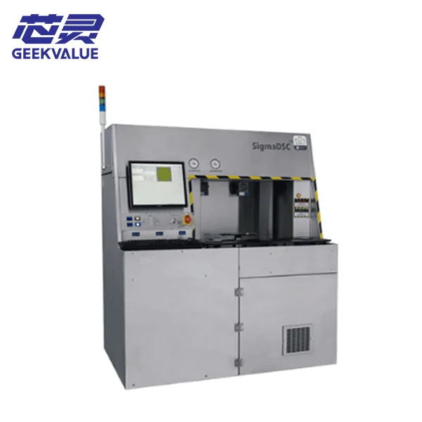
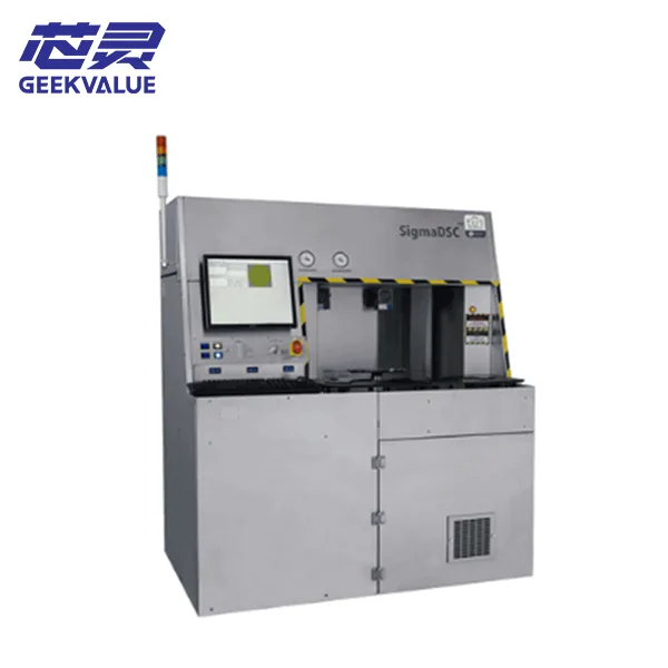
 The core positioning of the ThinkLaser SigmaDSC is that of a fully automated "Hard Marking" laser marking system—specifically designed for 100mm to 200mm (4 to 8-inch) wafers—that fully complies with Class 1 (ISO Class 3) cleanroom standards.
Its core value lies in utilizing laser technology with programmable depth control to create permanent, highly readable identification codes on wafers. These codes are engineered to withstand the rigors of subsequent high-intensity manufacturing processes—such as back-side thinning, high-temperature treatments, and chemical cleaning—thereby ensuring strict product traceability throughout its entire lifecycle.
**Core Principles**
The technological core of the SigmaDSC revolves around "Hard Marking":
**Dot-Matrix Thermal Marking:** This technique employs a focused, high-energy-density laser beam directed at specific locations on the wafer surface. This causes the material to instantly and locally melt or vaporize, forming physical indentations (pits) with a specific depth (up to 110 microns).
**Extreme Pulse Stability:** The key to achieving uniform hard marking lies in the laser source's exceptional pulse-to-pulse stability. ThinkLaser’s patented diode-pumped solid-state laser controls pulse stability to a level of <0.5% at a frequency of 1 kHz. This ensures a high degree of consistency in the depth and circularity of every single dot—serving as the cornerstone for guaranteeing an aspect ratio (major-to-minor axis ratio) of <1.1 and ensuring superior readability.
**Dual-Spot Optics™:** A critical design feature offering enhanced flexibility, this technology allows users to switch between two distinct spot sizes—ranging from 50µm to 110µm—via software control within the same system, thereby accommodating a variety of marking materials and application requirements.
**Core Advantages & Specifications**
The SigmaDSC is engineered to handle a wide range of substrate materials (including Silicon, Silicon Carbide, Gallium Arsenide, Gallium Nitride, Glass, Ceramics, etc.) and to withstand the demanding environments of semiconductor manufacturing. Its core performance parameters are clearly defined:
**Feature Category** | **Detailed Description / Specific Specifications**
**Hard Marking Capability** | **Programmable Depth Control:** Automatically adjusts marking depth, reaching up to 110 µm.
**Depth Accuracy:** ±10%.
**Throughput:** Up to 250 wafers per hour. Precision & Compatibility | Compatibility & Process: Compatible with 100mm to 200mm wafers, as well as 300mm/310mm panels.
Marking Accuracy: Within a 50x50mm area following wafer alignment, the repeatability is ±0.125 mm.
Broad Applicability: Suitable for a wide range of materials, including Silicon (Si), Silicon Carbide (SiC), Gallium Arsenide (GaAs), Gallium Nitride (GaN), and others.
Automation & Communication | Fully Automated Operation: Minimizes manual intervention and supports Open Cassette handling.
Factory Automation Interface: Supports SECS II/GEM protocols for seamless integration into factory MES systems.
Comprehensive System Monitoring: Precisely records all laser performance data down to the SPC (Statistical Process Control) level.
Hardware Specifications | Laser Type: Nd:YLF diode-pumped solid-state laser.
Laser Wavelength: 1053 nm.
Marking Location: Within a 25mm annular band from the wafer edge, allowing for the placement of multiple mark groups in any orientation.
Operating System: Windows 7 Pro SP1 (32-bit).
Industry Standards | SEMI Standards: Fully compliant with SEMI standards, supporting marking specifications such as T7, M12, and M13.
International Certifications: Compliant with safety and environmental standards including CE, SEMI S2, S8, and S14.
Key Functions & Applications
The SigmaDSC is primarily applied in semiconductor manufacturing environments where maintaining high traceability throughout the entire product lifecycle is critical:
Semiconductor Front-end Wafer Manufacturing: Immediately upon entering the cleanroom, a unique, permanent ID is inscribed on the wafer—an ID designed to withstand the rigors of all subsequent harsh processing steps (such as back-side thinning). This serves as the lifeline for quality traceability and Statistical Process Control (SPC) data throughout the entire production workflow—spanning silicon wafer manufacturing, foundries, and Integrated Device Manufacturers (IDMs).
Advanced Packaging: Provides reliable ID marking for Reconstituted Wafers or Panels within Fan-out Wafer-Level Packaging (Fan-out WLP) processes.
**Comparison of Complementary Equipment and Product Lines**
SigmaDSC constitutes a pivotal component within ThinkLaser’s comprehensive wafer identification solution. The SigmaClean system you mentioned serves as a distinct complement to it:
**Feature** | **SigmaDSC (Hard Marking)** | **SigmaClean (Soft Marking)**
**Core Process** | Hard Marking | Soft Marking
**Key Advantages** | Marks possess physical depth; capable of withstanding the most rigorous post-processing steps, such as mechanical grinding. | Debris-free with ultra-high cleanliness; meets the strictest cleanroom requirements.
**Typical Application Scenarios** | Used for wafers undergoing "hard" processes—such as back-side thinning—to provide permanent traceability. | Used in front-end wafer manufacturing environments where zero surface damage and extremely high cleanliness are paramount.
**Summary**
The ThinkLaser SigmaDSC is a fully automated laser marking system dedicated to providing ultra-durable "hard marking" for 200mm wafers. Its core technological advantages lie in its programmable depth control, Dual-Spot Optics™ technology, and SECS/GEM interface for full automation. Leveraging a stable laser system, closed-loop control, and advanced automation features, it ensures exceptional mark depth uniformity and circularity across a variety of substrate materials. Rather than performing cleaning or assembly tasks, it serves the critical function of providing global identity authentication for wafers.