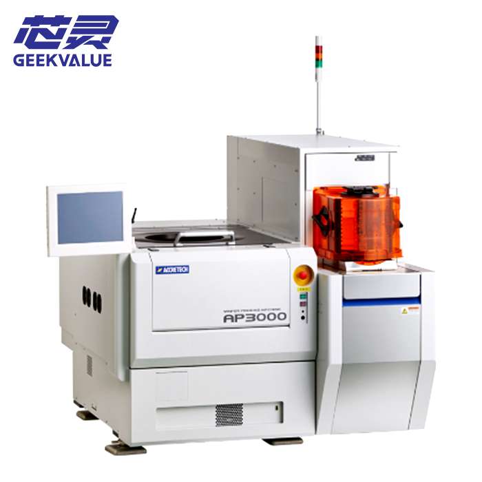
ave up to 70% on SMT Parts – In Stock & Ready to Ship
Get Quote →Professional probe station solutions for wafer-level testing, RF measurement, MEMS analysis, IC characterization, failure analysis, and semiconductor R&D. New, used, and refurbished systems are available for global customers.
A probe station is a precision testing system used to contact semiconductor wafers, dies, MEMS devices, RF chips, and microelectronic components with probe needles. It helps engineers perform electrical testing, device characterization, process verification, and failure analysis before packaging or mass production.
Used for semiconductor wafer inspection, electrical measurement, and device validation.
Supports accurate probe alignment for small pads, dies, and advanced devices.
Compatible with microscopes, analyzers, thermal chucks, RF probes, and test instruments.
Different semiconductor testing tasks require different probe station configurations. Whether you need manual operation for R&D, automatic wafer probing for production, RF testing for high-frequency devices, or thermal testing for reliability analysis, choosing the right system can improve testing accuracy, efficiency, and long-term equipment value.
Probe stations are widely used in semiconductor fabs, IC design companies, research institutes, universities, packaging houses, and failure analysis labs.
Talk to Our EngineerDifferent probe station systems can be configured according to wafer size, probing accuracy, chuck type, microscope requirement, RF testing condition, temperature range, and automation level.
Choose the system according to 2-inch, 4-inch, 6-inch, 8-inch, or 12-inch wafer testing needs.
Different applications such as RF, MEMS, IC testing, and failure analysis require different configurations.
Micron-level positioning accuracy is important for small pads, advanced dies, and high-density devices.
Manual systems suit labs and R&D, while automatic systems are better for production testing.
RF testing and temperature-controlled testing require special probes, chuck systems, and test setups.
New, used, and refurbished probe stations provide different cost and delivery advantages.
Probe station prices vary depending on brand, wafer size, automation level, RF capability, thermal chuck, microscope system, accessories, and equipment condition.
| Probe Station Type | Typical Price Range | Best For |
|---|---|---|
| Manual Probe Station | $3,000 – $20,000+ | R&D, labs, universities, low-volume testing |
| Semi-Automatic Probe Station | $20,000 – $80,000+ | Engineering verification and medium-volume testing |
| Automatic Probe Station | $80,000 – $300,000+ | High-throughput semiconductor production |
| RF Probe Station | Depends on RF setup | RF chips, microwave devices, 5G components |
| Refurbished Probe Station | Lower than new equipment | Cost-saving semiconductor testing projects |
The final price depends on actual configuration and available inventory. Contact us with your testing requirements for a more accurate quote.
We help customers source, inspect, and supply probe station systems from well-known semiconductor equipment brands according to testing requirements and budget.
Available models may change depending on inventory. Contact us to confirm current stock, configuration, condition, delivery time, and quotation.
Suitable for wafer probing, device characterization, and semiconductor lab applications.
Check AvailabilityProfessional choice for advanced wafer testing, RF probing, and high-precision applications.
Check AvailabilityUsed for semiconductor wafer testing, RF measurement, and laboratory testing environments.
Check AvailabilityAvailable for customers looking for cost-effective used semiconductor testing equipment.
Check AvailabilityCaused by probe wear, alignment error, dirty pads, or unsuitable probing force.
Often related to positioning accuracy, microscope setup, chuck flatness, or operator handling.
Requires proper RF probes, cables, calibration, grounding, and compatible probe station setup.
Thermal testing requires stable chuck control and suitable temperature compensation.
Precision probing may require vibration isolation, stable platform design, and proper installation.
Many customers choose unsuitable systems without considering wafer size, application, and test setup.
We support semiconductor manufacturers, universities, R&D centers, testing labs, packaging companies, and electronics companies that require reliable wafer testing equipment.
For customers requiring the latest configuration, long-term stability, and full equipment lifecycle support.
Cost-effective choice for labs, fabs, and manufacturers that need reliable testing equipment with lower investment.
Suitable for urgent projects, budget-sensitive purchases, and replacement needs.
We do not only sell equipment. We help customers select suitable probe station systems according to wafer size, test application, probing accuracy, RF requirement, thermal testing condition, budget, and delivery schedule.
Experienced in supplying semiconductor testing, packaging, and inspection equipment.
Each system can be checked, configured, and verified before export.
Export packaging, logistics support, and worldwide equipment delivery available.
Help customers match the right model based on testing purpose and technical requirements.
A probe station is used for wafer-level electrical testing, semiconductor device characterization, RF measurement, MEMS testing, and failure analysis.
A manual probe station is operated by hand and is suitable for R&D or low-volume testing. An automatic probe station offers higher throughput and is commonly used in production testing.
Yes. Used and refurbished probe stations are popular options for customers who want reliable wafer testing equipment with lower investment and faster delivery.
RF probe stations are designed for high-frequency device testing, microwave measurement, 5G components, RF chips, and advanced semiconductor applications.
The price depends on brand, wafer size, automation level, RF capability, thermal chuck, microscope system, accessories, and whether the equipment is new or refurbished.
You should consider wafer size, testing application, positioning accuracy, microscope requirement, RF compatibility, thermal chuck requirement, automation level, and budget.
Tell us your wafer size, application, preferred brand, manual or automatic requirement, RF or thermal testing needs, and budget range. Our team will recommend suitable equipment.
Why do so many people choose to work with GeekValue?
Our brand is spreading from city to city, and countless people have asked me, "What is GeekValue?" It stems from a simple vision: to empower Chinese innovation with cutting-edge technology. This is a brand spirit of continuous improvement, hidden in our relentless pursuit of detail and the delight of exceeding expectations with every delivery. This almost obsessive craftsmanship and dedication is not only the persistence of our founders, but also the essence and warmth of our brand. We hope you will start here and give us an opportunity to create perfection. Let us work together to create the next "zero defect" miracle.
DetailsContact a sales expert
Reach out to our sales team to explore customized solutions that perfectly meet your business needs and address any questions you may have.