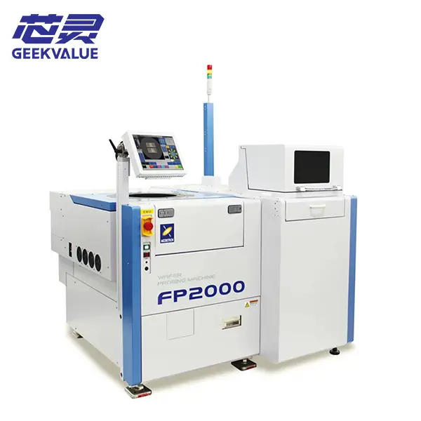
 The FP2000 is a 200mm (8-inch) fully automated wafer/frame dual-purpose prober** launched by ACCRETECH of Japan. It is primarily designed for CP testing of pre-diced chips on dicing frames, while also being compatible with standard 5–8 inch whole wafers. It is a mainstream model for testing CSP/WLCSP, MEMS, and ultra-thin/warped wafers.
I. Working Principle
The FP2000 is essentially a high-precision electrical testing and sorting device. Its core principle consists of three steps:
* **Automatic Loading, Unloading, and Positioning:** Supports automatic loading, alignment, and fixation of whole wafers or pre-diced wafers/chips attached to dicing frames.
* **Image Recognition and Precision Alignment:** A high-resolution camera and image processing software automatically recognize chip pads, driving the XYθ platform to move with high precision, ensuring the probe card tip is accurately aligned with the pad.
**Image Recognition and Precision Alignment:** A high-resolution camera and image processing software automatically recognize chip pads, driving the XYθ platform to move with high precision, ensuring the probe card tip is precisely aligned with the pad. Soft-landing Electrical Testing: Z-axis soft-landing control; the probe lightly presses against the pad to form an electrical connection; the ATE tester outputs a signal to test the chip's function/parameters, recording good/bad results and marking them.
Data Processing and Sorting: Automatically classifies and stores data according to test results, connecting to backend sorting/packaging equipment.
Core Technical Highlights: Equipped with a unique chip position correction algorithm, specifically compensates for the stretching, offset, and warping errors of the chip on the frame after dicing, ensuring precise probe contact.
II. Core Specifications (2026 Latest)
Table Item Parameter Applicable Size 5/6/8 inch (120/150/200mm) whole wafer; 8-inch dicing frame (compatible with 6-inch frame)
Positioning Accuracy XY: ±1.0 μm; θ: ±0.001°
Moving Speed XY: Maximum 200 mm/s; Z: Maximum 20 mm/s
Temperature Range Standard: Room temperature; Optional: -40℃ ~ +150℃ High and low temperature testing
Stage High-rigidity ceramic stage, vacuum adsorption; supports ultra-thin (≤50μm), high warp wafers/frames
Alignment System Dual camera (upper/lower) automatic alignment; magnification 200–1000×
Probe Card Compatible with all standard 200mm probe cards; automatic parallelism calibration
Capacity Typical: 200–300 wafers/day (8 1800mm dicing frame; Multi-Die optional
Dimensions/Weight: Approx. 1800×1200×1800 mm; Approx. 1800 kg
III. Main Functions
One-click wafer/dicing frame switching
No hardware modification required, one-click switching between whole wafer and dicing frame modes significantly reduces changeover time.
Fully automated testing process
Automatic loading → Image alignment → Probe contact → Electrical testing → Result recording → Automatic unloading, fully unattended.
High-precision position correction
Dedicated software compensates for chip stretching, offset, and warping after dicing, improving yield by 3–5%.
Wide temperature and special testing
Optional high and low temperature, micro-current, high voltage, and RF test modules, covering MEMS, power devices, and automotive electronics needs.
Needle Track monitoring
Real-time monitoring of probe wear and bending, preventing pad damage and reducing maintenance costs.
Multi-Die parallel testing
Supports simultaneous testing of up to 4 chips, increasing throughput by 2–3 times. Data Traceability and Management: Barcode/QR code recognition, ID reading and writing, real-time upload of test data, and support for yield analysis and traceability.
Data Traceability and Management: Barcode/QR code recognition, ID reading and writing, real-time test data upload, supporting yield analysis and traceability.
IV. Core Functions: Mainstay equipment for chip testing (CP): Performs 100% electrical testing on chips already cut on the wafer frame after dicing and before packaging, screening for good products and avoiding packaging waste.
Advanced Packaging Adaptation: Designed specifically for CSP/WLCSP, Fan-out, and 2.5D/3D packages, solving testing challenges related to ultra-thin/warpage/dicing.
Dedicated for MEMS/Power Devices: Supports high-precision testing of MEMS (pressure/accelerometer/gyroscope), MOSFETs, IGBTs, and diodes/transistors.
Improved Yield and Capacity: Automatic calibration + high-speed testing + parallel processing improve yield, double capacity, and reduce unit testing costs.
V. Key Advantages (Comparison with Similar Products)
1. Unique "Wafer/Frame Dual-Use" High-Precision Model: Most competing products are dedicated to either wafers or frames only; the FP2000 is equivalent to two machines in one, offering extremely high cost-effectiveness.
2. Industry-Leading Post-Dieting Testing Accuracy: Utilizing a unique 20-year-old frame testing algorithm, it compensates for dicing stretching/warping, achieving ±1μm positioning accuracy, far exceeding competitors' ±2–3μm.
3. Strong Capability for Handling Ultra-Thin/Warped Wafers: Vacuum adsorption + flexible support ensures stable handling of wafers ≤50μm ultra-thin and >5mm warped, with yield loss <1%.
4. Mature, Stable, and Low TCO: Based on the UF2000 high-end platform, with over 1000 units installed globally, the mean time between failures (MTBF) is >5000 hours, resulting in low maintenance costs.
5. Modular Expansion, Flexible Adaptation: Optional modules for high and low temperature, high pressure, micro-current, RF, multi-chip parallel processing, probe cleaning, etc., allowing for upgrades as needed and protecting investment.
6. Simple Operation, Easy to Learn: Unified GUI interface, one-click mode switching, automatic alignment, and automatic testing; even beginners can learn to use it in one day.
VI. Typical Application Scenarios
CSP/WLCSP Production Line: 8-inch dicing and frame testing, high-volume, high-yield
MEMS Manufacturing: Pressure/accelerometer/gyroscope chips, high and low temperature + micro-current testing
Power Devices: MOSFETs, IGBTs, diodes, high-voltage/high-current testing
Ultra-thin Wafers: Logic/analog chips below 50μm, back-side adsorption + warpage compensation
Automotive Electronics: AEC-Q100 certification, wide temperature range (-40℃~150℃) + high reliability testing
VII. Comparison with Competitors (Quick Overview)
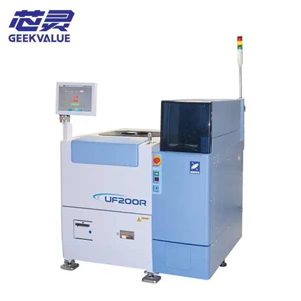
Table Comparison Item ACCRETECH FP2000 TEL Precio octo UF200R
Wafer/Frame Dual Use Native Support Wafer Only Wafer Only
Diceing Accuracy ±1μm (calibrated) ±1.5μm (uncalibrated) ±1.5μm (uncalibrated)
Ultra-thin Processing ≤50μm ≥100μm ≥75μm
Capacity (8-inch frame): 200–300 wafers/day
Frame not supported
Price: Medium-high, Medium, Low
Applicable Scenarios: Frame + Wafer, Advanced Packaging, Pure Wafer, General Mass Production, Pure Wafer, Cost-Effective Mass Production
In short: The FP2000 is the only all-around probe station in the 8-inch market that can handle both "whole wafer" and "diced frame" high-precision testing. It is especially suitable for advanced applications such as CSP/WLCSP, MEMS, and ultra-thin wafers, and is the absolute mainstream model for frame testing globally from 2020 to 2026.