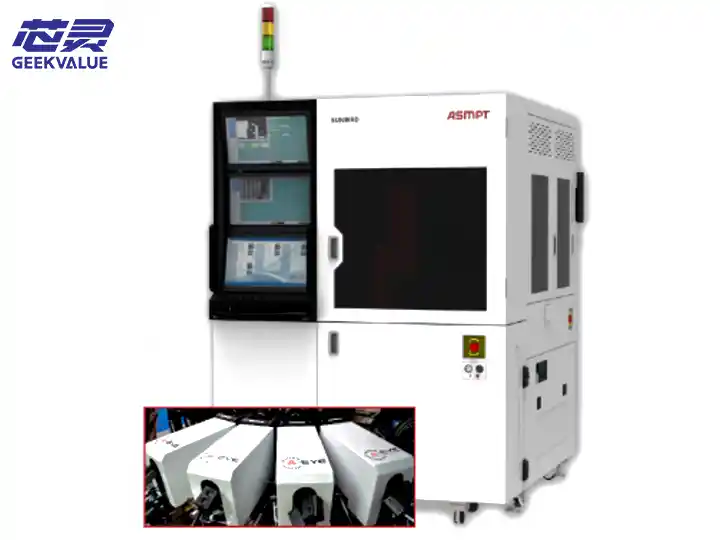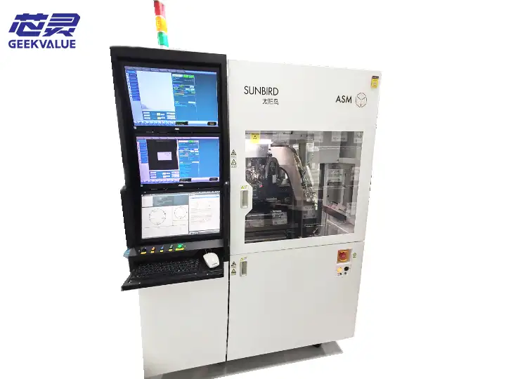
SUNBIRD is an efficient, high-precision, fully automatic turret-based wafer-level test system designed for the semiconductor manufacturing industry. It is mainly used for electrical testing of wafers before cutting (wafer sort/CP test). Its core advantages are high throughput, high stability, and modular design. It can adapt to a variety of test requirements from R&D to mass production, especially suitable for large-scale testing scenarios of high-density integrated circuits (such as logic chips, memory, sensors, etc.).
2. Core features and technological innovations
2.1 Turret-Based Design
Parallel testing capability: Through the multi-station turret design, parallel loading and unloading, alignment, and testing of wafers are achieved, significantly improving efficiency (such as an 8-station turret can process multiple wafers at the same time).
Non-stop operation: When the turret rotates to switch stations, other stations continue to operate, eliminating the waiting time of traditional testers.
2.2 Fully automated integration
Robot collaboration: Integrate high-precision robotic arms and visual positioning systems to automatically complete wafer loading, alignment, probe contact and sorting.
Intelligent scheduling algorithm: optimize test sequence and path, maximize equipment utilization (UPH can reach 200+ pieces/hour, depending on test complexity).
2.3 High-precision test capability
Nano-level positioning accuracy: laser interferometer or high-resolution encoder is used to ensure the alignment accuracy of probe card and wafer pad (within ±1μm).
Multi-channel test: supports parallel testing of up to thousands of channels, compatible with DC/AC parameters, RF, mixed signal testing, etc.
2.4 Flexibility and scalability
Modular design: temperature control module (-55°C~150°C), multi-DUT test board, different probe card interfaces (such as MEMS probe) can be selected according to needs.
Software open interface: supports integration with third-party EDA tools (such as Cadence, Keysight) and MES systems to achieve real-time data analysis (SPC, Bin Map generation).
2.5 Reliability and maintainability
Self-diagnosis system: real-time monitoring of probe wear, temperature drift and other parameters, triggering automatic calibration or alarm.
Quick line change: Standardized fixture design supports fast replacement of probe cards/test boards (changeover time < 10 minutes).
3. Typical application scenarios
Logic/memory chip mass production test: such as efficient CP test of SoC, DRAM, and NAND Flash.
High-precision sensor test: multi-parameter verification of MEMS devices (gyroscopes, pressure sensors).
Third-generation semiconductor testing: adapt to the high-voltage and high-temperature test requirements of SiC/GaN wafers.
4. Technical parameter example (adjustable according to actual configuration)
Item Parameter
Wafer size 6"/8"/12" (customizable)
Number of test stations 4/6/8 stations optional
Positioning accuracy ±0.5μm @ 3σ
Test temperature range Normal temperature ~ 150°C (optional low temperature module)
Maximum number of test channels 2048 channels (expandable)
Communication interface GPIB/Ethernet/SECS/GEM
5. Market competitiveness analysis
Advantages:
Compared with single-station testers (such as traditional Prober), efficiency is improved by 30%~50%.
Strong compatibility, supporting seamless transition from low throughput in R&D to high throughput in mass production.
Comparison products:
Competes with Tokyo Electron (TEL) Prober, Teradyne UltraFlex, etc., but has more distinctive features in turret architecture and cost-effectiveness.
6. Customer Value
Reduced testing costs: High throughput reduces the number of equipment investments.
Improved yield: High-precision testing and real-time data feedback help optimize the process.
Future adaptability: Supports AI-driven test optimization and advanced packaging (such as Chiplet) testing requirements.
7. Summary
SUNBIRD provides an efficient, reliable and flexible wafer testing solution for the semiconductor industry through innovative turret design, full automation and high-precision testing capabilities, especially for advanced process chip manufacturers pursuing mass production efficiency and data quality. Its modular architecture also reserves upgrade space for future technological evolution.