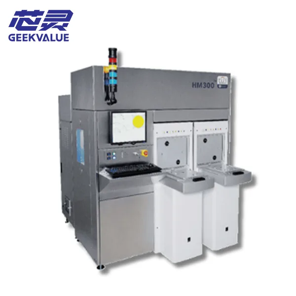
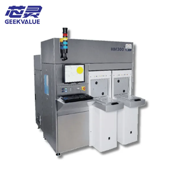
 The ThinkLaser HM300 is a fully automated "Hard Marking" laser marking machine, specifically engineered to meet the rigorous deep-marking requirements—known as "hard marking"—inherent in the semiconductor wafer manufacturing process. Its core value lies in its ability to engrave permanent identification codes onto wafers through a programmable depth control function; these codes are robust enough to withstand the abrasive stresses generated by subsequent high-intensity manufacturing processes, thereby ensuring complete product traceability throughout its entire lifecycle—from chip fabrication and packaging through to final testing.
**Core Technologies and Key Specifications**
The technological core of the HM300 revolves around three fundamental elements: depth, precision, and automation. Its specific technical specifications are as follows:
**Item** | **Specification / Description**
**Equipment Type** | Fully Automated Hard Marking Laser Marking System
**Target Application** | Specifically designed for semiconductor wafer hard marking, complying with relevant requirements of SEMI standards
**Core Functionality** | Programmable Depth Control: Adjustable marking depth, reaching a maximum depth of 110 microns (µm), with a depth accuracy of ±10%
**Core Technology** | Dual-Spot Optics™: Employs a dual-beam optical design that allows for software-controlled switching between two distinct laser spot sizes (ranging from 50 µm to 110 µm) within the same system
**System Monitoring** | Comprehensive System Monitoring: Accurately records all laser performance data
**Automation Interface** | Supports SECS II/GEM interfaces to facilitate factory automation management
**Wafer Compatibility** | Supports 100mm to 200mm wafer sizes (optional support for 300mm/310mm panels available; feasibility confirmed via existing data)
**Functions, Advantages, and Features**
Leveraging a suite of advanced technologies, the HM300 effectively addresses the core pain points within the field of wafer marking:
**"Hard Marking" Capability for Rigorous Processes:** Unlike "Soft Marking," the HM300's "Hard Marking" capability generates marks of sufficient depth. This ensures that the marks remain intact—without degradation or abrasion—throughout subsequent high-intensity processes (such as high-temperature treatment, chemical cleaning, and mechanical grinding), thereby maintaining complete process traceability. **High Precision and Flexibility:**
**Controllable Depth:** The programmable depth control function (offering an accuracy of up to ±10% and a depth range reaching 110 µm) empowers customers to precisely fine-tune the marking depth, ensuring a perfect match with specific process requirements. **Adjustable Spot Size:** Its patented Dual-Spot Optics™ technology enables software-controlled switching between two laser spot sizes (50 µm and 110 µm) without requiring any hardware modifications, thereby accommodating a diverse range of marking materials and specific aesthetic requirements.
**Automation and Intelligent Management:**
**Fully Automated Operation:** Offers fully automated equipment operation capabilities, minimizing human intervention and reducing the potential for errors.
**SECS/GEM Protocol Support:** Supports industry-standard automation protocols (SECS II/GEM), allowing for seamless integration into the Manufacturing Execution Systems (MES) of modern semiconductor fabs to enable real-time equipment status monitoring and remote management of process parameters.
**Comprehensive Data Logging:** The system accurately records all laser performance data, providing a solid foundation for process analysis and quality traceability.
**Broad Material and Process Compatibility:**
Designed specifically for customers working in the fields of compound semiconductors, advanced process nodes, and advanced packaging, this system effectively addresses the marking challenges associated with next-generation semiconductor materials such as SiC, GaN, and GaAs.
Its design philosophy extends far beyond basic marking tasks; it is positioned as a "comprehensive wafer marking solution," capable of undergoing customized evaluations and upgrades—tailored to unique wafer materials and dimensions—to meet specific requirements.
**Application Areas**
The HM300 is a critical piece of equipment in the fields of semiconductor manufacturing and advanced packaging, primarily applied in the following areas:
**Semiconductor Manufacturing (Front-end and Back-end):** Provides high-integrity permanent IDs for substrate wafers—including silicon, SiC, and GaN—thereby supporting automated line management and quality traceability within fabrication plants (Fabs) and assembly/test facilities.
**Advanced Packaging:** Delivers reliable marking for reconstructed wafers or panels within Wafer-Level Packaging (WLP) and Panel-Level Packaging (PLP) processes.
**Synergy with Other ThinkLaser Products**
ThinkLaser offers a comprehensive suite of wafer marking solutions, within which the HM300 plays a pivotal role:
**Synergy with Soft Marking Equipment:** On the same production line, the HM300 can operate in tandem with ThinkLaser’s SC300 (a soft marking system for 300mm wafers) or SigmaClean (a soft marking system for 100–200mm wafers). Manufacturers can flexibly select the most suitable marking technology based on specific process nodes or customer requirements.
**Summary**
In summary, the ThinkLaser HM300 is a specialized, industrial-grade system fundamentally designed to provide depth-controlled, permanent wafer marking that meets the most rigorous industry standards. Through its programmable depth control, dual-beam technology, and advanced automation capabilities, it effectively resolves the critical challenge within the semiconductor industry of maintaining product traceability throughout high-intensity process chains; it stands as a key piece of equipment in high-end wafer manufacturing and packaging lines. Its developer, ThinkLaser, boasts over 80 years of collective team experience in this field and holds an approximate 80% market share within the United States.