
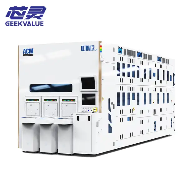
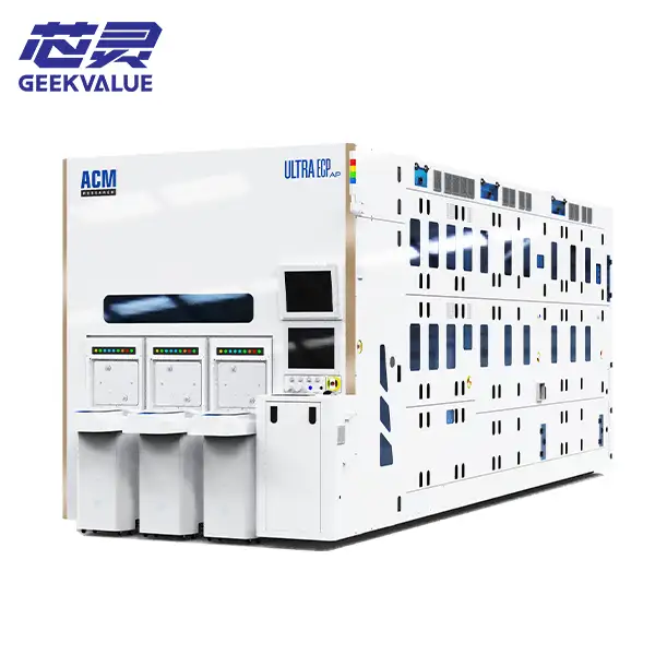
 ACM Research’s ULTRA ECP ap-p is a groundbreaking panel-level horizontal plating system, distinguished by its core value: filling a critical process gap in the industrialization of Fan-Out Panel-Level Packaging (FOPLP).
As the first commercialized, mass-production copper deposition system designed for the large-panel market, it aims to facilitate a seamless transition for advanced packaging from the 300mm wafer level to the more cost-effective panel level. Leveraging its patented horizontal plating technology, exceptional uniformity, and effective management of warped panels, the system achieves processing performance comparable to that of circular wafer processes, thereby meeting the rigorous manufacturing demands of next-generation devices such as AI GPUs and high-density HBMs.
The following is a comprehensive overview of the ULTRA ECP ap-p, compiled based on publicly available information:
**Equipment Positioning**
**Product Series:** Panel-level (ap-p) model within the ULTRA ECP (Electrochemical Plating) platform.
**Industry Recognition:** Recipient of the 2025 "3D InCites Technology Enabling Award."
**Core Technologies and Features**
The technical highlights of the ULTRA ECP ap-p are as follows:
**Horizontal Plating Design:** Employs ACM’s patented horizontal plating technology—a departure from traditional vertical plating—which ensures exceptional uniformity in plating thickness across the entire panel through the synchronized rotation of the chuck and a rotating rectangular electric field. This approach also effectively minimizes chemical cross-contamination between process chambers; furthermore, the horizontal chamber design facilitates easier maintenance of individual chambers, thereby enhancing overall equipment efficiency.
**Optimized Precision Hardware:** Features a four-sided sealed dry-contact chuck, which enhances the reliability and cleanliness of wafer/panel handling. The copper plating chamber is equipped with high-speed plating paddles specifically designed for high-bump applications, enabling the formation of bumps exceeding 300 microns in height.
**Multi-Metal Support and Cross-Contamination Control:** Offers the flexibility to process a variety of metal materials—including copper, nickel, tin-silver, and gold—while utilizing in-chamber cleaning functions to minimize cross-contamination between different metal plating baths.
**Compatibility and Automation:** Supports both organic and glass substrates. Its automation system is specifically optimized for large panels—including critical operations such as panel flipping—achieving a level of efficient process control comparable to the standards established in wafer-level processing. Detailed Specifications
Based on publicly available information, the key specifications are as follows:
Panel Size: Supports a standard size of 510mm x 515mm, with an optional expansion capability up to 600mm x 600mm.
Process Compatibility: Supports electroplating steps within various processes, including Pillar, Bump, and Redistribution Layer (RDL) formation.
Capacity Configuration: Configurable with up to 16 plating chambers, complemented by 2 pre-wet chambers and 2 cleaning chambers to ensure optimal throughput.
Warpage Management: Capable of effectively processing panels with warpage levels of up to 7mm (approximately 10mm), a critical capability for advanced packaging processes.
Performance Metrics:
Within-Panel Uniformity (WIWU): < 5% ((max-min)/2Ave.)
Within-Die Uniformity (WIDU): < 5% ((max-min)/2Ave.)
Repeatability: < 3%
Key Application Areas
Primarily targets advanced semiconductor packaging applications, including but not limited to:
Fan-Out Panel-Level Packaging (FOPLP)
Pillar and Bump fabrication, as well as Redistribution Layer (RDL) formation
Through-Silicon Via (TSV) and Through-Glass Via (TGV) filling
High-Density Fan-Out (HDFO) products
Market Position and Competition
The ULTRA ECP ap-p holds a significant leading position in the emerging market for panel-level electroplating. Its primary competitors are major international semiconductor equipment manufacturers—such as Applied Materials and Lam Research—that are also developing panel-level packaging (PLP) electroplating solutions. ACM's key advantage lies in its status as a pioneer, having been the first to successfully deliver commercialized equipment in this field.
Summary
In summary, ACM Research's ULTRA ECP ap-p represents a forward-looking technology platform. It serves not only as a pivotal enabler in the advanced packaging industry's critical transition from "round wafers" to "rectangular panels," but also provides innovative solutions for enhancing the production efficiency and cost-effectiveness of high-end semiconductor devices, such as AI chips.