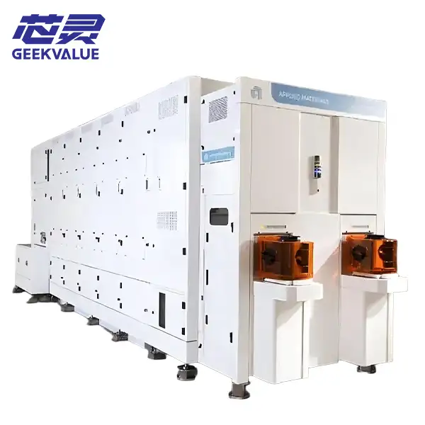
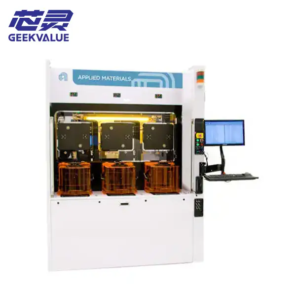
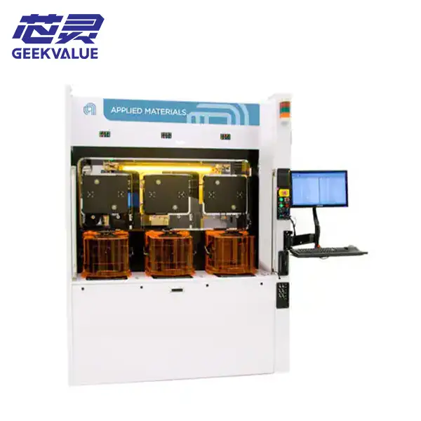
 Applied Materials' Raider® Edge ECD system stands as a benchmark in the field of electrochemical deposition (ECD) within semiconductor manufacturing. Resulting from the technological integration following Applied Materials' acquisition of Semitool, the system is widely deployed in advanced packaging and wafer-level interconnect processes, distinguished by its high flexibility, high throughput, and exceptional process control.
**System Positioning**
**Company:** Applied Materials, Inc.
**Product Model:** Raider® Edge ECD
**Equipment Type:** Automated Multi-Chamber Single-Wafer Electrochemical Deposition System
**Historical Significance:** An "Industry Benchmark" renowned in the field of single-wafer plating technology. It represents the fourth generation of single-wafer ECD tools; its predecessor, the Raider GT system, was originally designed to support the development of three generations of chip technology.
**Core Principles**
Electrochemical deposition involves utilizing an electric current to reduce metal ions onto a wafer surface, thereby forming a specific thin film. The Raider Edge ECD system goes beyond simple plating; through a sophisticated control system, it enables this process to achieve atomic-level precision. Furthermore, the system supports various wet processing steps, such as wafer etching and cleaning.
**Features and Advantages**
Its power lies not merely in its capability to handle standard plating tasks, but more significantly in its exceptional flexibility, precise process control, and highly automated design.
**Feature/Advantage** | **Detailed Description**
**Process Flexibility** | Capable of processing various wafer sizes, including 150mm, 200mm, and 300mm; supports multi-step wet processing sequences on wafers, including metal deposition, etching, and cleaning.
**Broad Material Support** | Supports the deposition of a wide range of metals and alloys, such as copper, nickel, gold, tin-silver, magnetic alloys, and gold-tin eutectic solders. It also supports multi-layer stack etching for specialized materials like CZT and AlN.
**Advanced Process Control** | Employs a multi-zone anode array to achieve uniform plating, even on ultra-thin or resistive seed layers. On 300mm wafers, its enhanced chamber reactor can dynamically adjust current density to ensure deposition uniformity.
**High Throughput & Low Cost** | "Teachless" precision automation eliminates downtime associated with manual calibration, while ion membrane technology extends chemical bath life, resulting in extremely low operating costs. Additionally, its compact footprint effectively boosts overall production capacity. **Proprietary Technology Expansion:** Its predecessor, the Raider GT system, supported up to six plating chambers and offered optional annealing or metrology modules, as well as integrated chambers for wafer edge, bevel, and backside cleaning.
**Application Areas**
**Advanced Packaging & Interconnects:** Used for copper interconnect filling in chip manufacturing, ensuring void-free filling; also utilized for the deposition of copper pillars, solder bumps (including lead-free solder), and redistribution layers (RDL) in wafer-level packaging.
**Specialty Device Manufacturing:** Used for multi-layer metal deposition in devices such as MEMS and sensors; provides high-quality copper filling for TSVs (Through-Silicon Vias) and TGVs (Through-Glass Vias).
**Power & Compound Semiconductors:** Used for thick copper deposition in power devices, as well as for low-stress backside metallization on thin wafers.
**Other Specialty Processes:** Capable of depositing gold via liners or cleaning glass wafers using ozone-based compounds; can perform multi-layer stack etching—going beyond traditional UBM (Under Bump Metallization) etching capabilities.
**Technical Specifications**
**Wafer Size Support:** 150mm, 200mm, 300mm
**Number of Plating Modules:** Base models support multiple modules; high-end models can accommodate up to 6.
**Plating Uniformity:** Industry-leading (specific data not provided).
**Supported Materials:** Cu (Copper), Au (Gold), SnAg (Tin-Silver), Ni (Nickel), magnetic alloys, AuSn (Gold-Tin Eutectic), etc.
**Process Capabilities:** Supports thick copper deposition up to 100µm, filling of High Aspect Ratio (HAR) structures, and filling for nodes with Critical Dimensions (CD) smaller than 22nm.
**Automation Level:** Fully automated, cluster-based multi-chamber architecture; supports factory automation protocols such as SECS/GEM; compatible with SMIF and FOUP wafer transfer pods.
Comparison with the ACM ULTRA ECP ap-p
As a key player in the field of semiconductor plating equipment, this system is positioned quite differently from the ACM Research ULTRA ECP ap-p—the model you inquired about previously. The choice between the two ultimately depends on your specific process requirements.
**Comparison Dimensions** | **Applied Materials Raider Edge ECD** | **ACM Research ULTRA ECP ap-p**
**Core Technology** | Focuses on high-precision plating on single wafers | Breakthrough horizontal plating technology for panel-level substrates
**Target Substrate** | 150mm – 300mm wafers | 510mm x 515mm panels
**Core Advantages** | Industry benchmark; high technological maturity; wide process window | Fills an industry gap; enables cost-effective mass production at the panel level
**Process Focus** | Emphasizes seamless integration with front-end interconnect processes | Specifically designed for Fan-Out Panel-Level Packaging (FOPLP)
The true strength of the Raider Edge ECD lies in its evolution: originally a technology utilized for copper interconnects at the 22nm node, it has transformed into a highly versatile platform capable of supporting a wide array of specialized processes—ranging from magnetic materials to advanced packaging—thereby demonstrating its profound scalability.