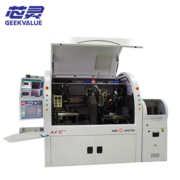
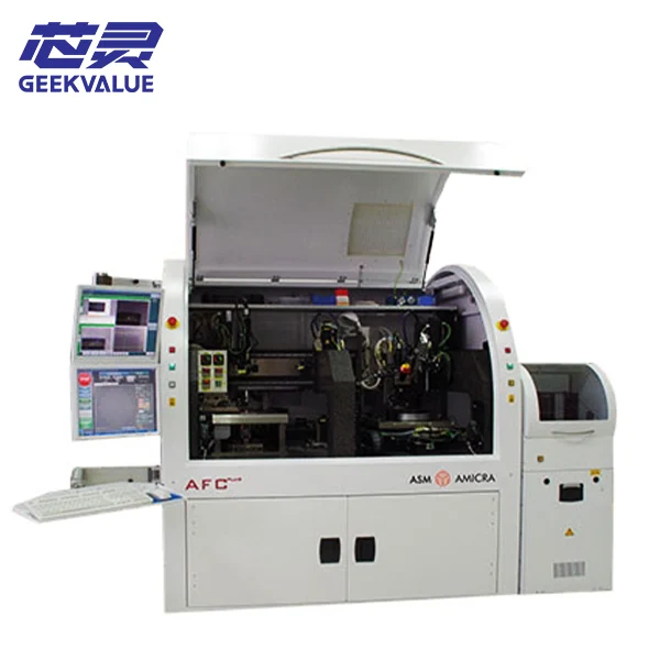
 The ASM AFC Plus is a technologically mature, ultra-high-precision Flip Chip Bonder. In practice, it serves as a versatile dual-purpose system—capable of both standard die bonding and flip-chip bonding—renowned for its stable precision of ±1.0 µm and robust process adaptability. It is a highly popular choice for R&D applications and the low-volume production of high-end products.
Core Specifications: High Precision & Multifunctionality
Feature | Detailed Description
Equipment Type | Fully Automatic Die Bonder / Flip Chip Bonder
Core Precision | Alignment/Placement Accuracy: ±1.0 µm @ 3σ
Cycle Time (Per Die) | Approx. < 15 seconds
Die Size | Extremely wide range supported: from 0.1 mm to 20 mm
Substrate/Wafer Size | Capable of handling substrates or wafers up to 300 x 300 mm
Bonding Force Range | Finely controllable, ranging from 10g to 2kg
Compatible Processes | - Eutectic Bonding
- Epoxy Dispensing
- UV Curing
- Laser Bonding
Alignment Method | Standard configuration features Passive Alignment; upgradable to Active Alignment upon request.
How is its Flexibility Demonstrated?
The key to the AFC Plus lies in its modular design: it can function as a standard Die Bonder, yet can be reconfigured to operate as a Flip Chip Bonder.
Key Integration: The core component enabling the flip-chip functionality is the "Flip Chip Option" module. This module allows the system to flip the die, placing it with its active side facing downward.
Material Compatibility: Supports a wide array of bonding processes—including eutectic, epoxy dispensing, UV curing, and laser bonding—accommodating various flip-chip materials.
High Versatility: Its high degree of modularity and flexibility make it one of the most adaptable die bonders currently available on the market, capable of covering a broad spectrum of assembly scenarios, ranging from die-to-wafer to die-to-substrate bonding. Core Application Areas
Leveraging its ultra-high precision and process flexibility, the AFC Plus primarily serves high-value applications with stringent requirements for bonding quality:
Silicon Photonics: Boasts a distinguished track record in cutting-edge fields such as optical communication transceivers and optical engines.
Advanced Packaging: Suitable for high-end semiconductor packaging applications, including 3D integration and die stacking.
MEMS (Micro-Electro-Mechanical Systems): Enables the precision assembly of sensors such as accelerometers and gyroscopes.
Optical Devices: Encompasses LiDAR, VCSELs, WDM (Wavelength Division Multiplexing) devices, microlenses, and more.
R&D and Prototyping: Widely utilized in numerous advanced research facilities and university laboratories due to its exceptional flexibility and precision.
In summary, the application scenarios for the AFC Plus differ markedly from those of the previously discussed SHIBAURA TFC-9000: while the TFC-9000 caters to large-scale mass production, the AFC Plus specializes in ultra-high precision, high-mix, and flexible manufacturing—making it the ideal tool for the R&D and production of advanced packaging and cutting-edge optoelectronic devices.