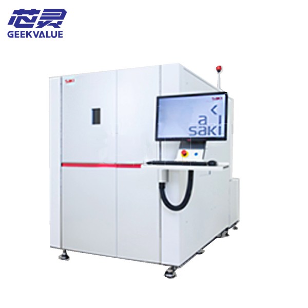
SAKI BF-3Si-L2 is an advanced 3D solder paste inspection system (3D SPI, Solder Paste Inspection) designed for modern SMT (surface mount technology) production lines. It uses high-precision 3D imaging technology to quickly and accurately detect the printing quality of solder paste before reflow soldering, including key parameters such as volume, height, area, offset, etc., so as to effectively prevent soldering defects and improve production yield.
2. Core advantages
✅ Ultra-high precision detection
Micron-level measurement: Z-axis (height) accuracy can reach ±1μm, suitable for ultra-fine pitch components such as 01005 and 0.3mm pitch BGA.
Full 3D modeling: Through multi-angle scanning, the volume, height, and shape of the solder paste are accurately calculated to avoid the misjudgment problem of traditional 2D SPI.
✅ High-speed detection, suitable for high-capacity production lines
The detection speed is up to 600mm/s, and dual-lane mode is supported to meet the needs of high-speed SMT production lines (such as mobile phones and automotive electronics production lines).
Intelligent motion control algorithm reduces mechanical vibration and ensures scanning stability.
✅ Intelligent algorithm reduces false alarm rate
AI deep learning: automatically optimizes detection parameters to adapt to different solder paste types (such as lead/lead-free, water-washable/clean-free).
Adaptive threshold analysis: reduces misjudgment caused by PCB reflection and color difference.
✅ Modular design, flexible expansion
Optional automatic cleaning module to reduce the impact of solder paste residue on detection.
Support linkage with AOI, placement machine, and MES system to achieve closed-loop control of intelligent manufacturing.
3. Technical principle
📌 3D imaging technology
BF-3Si-L2 adopts dual technology of laser triangulation + structured light projection:
Laser scanning: High-precision laser line is projected onto the solder paste surface, and the reflected light is captured by CCD camera to calculate height data.
Structured light assistance: Multi-angle stripe light projection enhances the 3D contour restoration ability of complex pads (such as BGA, QFN).
📌 Inspection process
PCB positioning: High-precision linear motor drive to ensure accurate scanning position.
3D scanning: Laser + structured light synchronously collect solder paste data.
AI analysis: Compare standard solder paste models to identify defects such as insufficient solder, bridging, offset, and abnormal shape.
Data feedback: Generate SPC reports in real time to guide printing process optimization.
4. Core functions
🔹 3D parameter detection of solder paste
Volume: Ensure that the amount of solder paste meets the standard to avoid cold soldering or short circuits.
Height: Detect the uniformity of solder paste to prevent collapse or poor molding.
Area: Analyze the coverage of solder paste and identify offset or diffusion anomalies.
Shape: Detect irregular shapes such as pull tips and depressions.
🔹 Defect detection capability
Defect type Detection principle
Insufficient Volume/height below threshold
Bridging Abnormal connection of adjacent solder paste heights
Misalignment The position deviation between solder paste and pad exceeds the allowable range
Shape Defect 3D contour does not conform to the standard model
5. Hardware and specifications
📌 Optical system
Laser source: 650nm red laser, accuracy ±1μm (Z axis), ±5μm (X/Y axis).
Camera: High-resolution 12MP CCD, supports high-speed scanning.
Light source: Multi-angle ring LED + coaxial light, adaptable to different PCB surfaces (high reflective, matte).
📌 Mechanical structure
Motion system: high-precision linear motor, repeatable positioning accuracy ±3μm.
Frame: High-rigidity aluminum alloy, anti-vibration design to ensure stability.
Autofocus: adapt to different PCB thicknesses (0.2mm~6mm).
📌 Technical Specifications
Parameters BF-3Si-L2 Specifications
Detection accuracy (Z axis) ±1μm
Detection speed Up to 600mm/s (single track), dual track mode optional
Minimum detection component 01005 (0.4mm × 0.2mm)
PCB size range 50mm × 50mm ~ 510mm × 460mm
Communication interface SECS/GEM, TCP/IP, RS-232
Power requirement AC 200-240V, 50/60Hz
6. Summary
SAKI BF-3Si-L2 3D SPI provides SMT production lines with high-precision, high-efficiency, and low false alarm solder paste detection solutions through laser + structured light dual 3D imaging, AI intelligent algorithm and high-speed scanning technology. Its core value lies in:
Preventing soldering defects: intercepting defects before reflow soldering and reducing rework costs.
Improving process control: optimizing printing parameters through real-time SPC data.
Adapt to future needs: support miniaturized components (01005, 0.3mm BGA) and high-mix production lines.
Recommended industries:
✔ Consumer electronics (mobile phones, tablets)
✔ Automotive electronics (ADAS, ECU)
✔ High-end manufacturing