SAKI 3Si-LS3EX is a high-performance 3D solder paste inspection equipment (SPI, Solder Paste Inspection), designed for high-precision SMT (surface mount technology) production lines. It is used to automatically detect key parameters such as volume, height, shape, offset, etc. of solder paste after printing and before patching to ensure stable printing process and reduce soldering defects after reflow soldering.
1. Equipment Overview
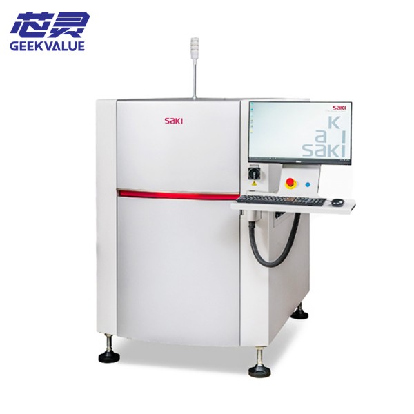
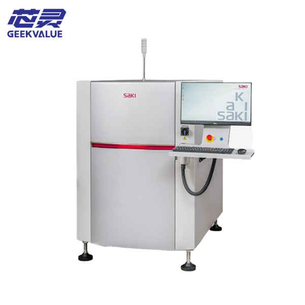
Model: SAKI 3Si-LS3EX
Type: 3D SPI (Laser Scanning Solder Paste Inspection System)
Core Application:
Detect solder paste printing quality (less tin, more tin, bridge, pull tip, offset, etc.).
Provide SPC (Statistical Process Control) data to optimize printing process.
Link with printers (such as DEK, MPM) to achieve closed-loop control.
2. Core Technology & Hardware Configuration
(1) 3D Imaging Technology
Laser Triangulation:
Use high-precision laser scanning to measure the height, volume, area, and coplanarity of solder paste.
Z-axis resolution ≤1μm, capable of detecting ultra-small component pads such as 01005 (0.4mm×0.2mm).
Multi-spectral auxiliary lighting (optional):
Combined with RGB+infrared light source, it enhances the contrast between solder paste and PCB and improves detection stability.
(2) High-speed detection system
Detection speed:
20~60cm²/s (depending on the accuracy requirements, up to 10μm resolution).
Motion control:
Use high-precision linear motor to ensure scanning stability and repeatability.
Supports dual-track detection (optional) to improve production line throughput.
(3) Intelligent software platform
SAKI VisionPro or AIx (AI enhanced version):
Real-time SPC analysis: Automatically calculate Cpk/Ppk and monitor solder paste printing stability.
AI defect classification: Automatically identify defects such as insufficient tin, bridging, and pulling tips to reduce the misjudgment rate (<1%).
Closed-loop control: Linked with printers (such as DEK, MPM) to automatically adjust scraper parameters.
3. Core detection capabilities
(1) Solder paste 3D parameter measurement
Detection items Measurement parameters Typical defects
Height Solder paste thickness (μm) Insufficient tin, excessive tin
Volume Solder paste volume (mm³) Insufficient tin, solder paste diffusion
Area Solder paste coverage area (mm²) Offset, bridging risk
Shape Solder paste contour (3D modeling) Pulling tips, collapse
(2) Compatibility
PCB size: Maximum support 510mm × 460mm (customizable).
Component range:
Minimum detection 01005 (0.4mm×0.2mm) pad.
Supports high-density packaging such as BGA, QFN, CSP, Flip Chip, etc.
Steel mesh type:
Applicable to step steel mesh, nano-coated steel mesh, electroformed steel mesh, etc.
4. Core advantages
(1) Comparison with 2D SPI
Comparison items SAKI 3Si-LS3EX (3D SPI) Traditional 2D SPI
Detection dimensions 3D (height + volume) 2D (area only)
Solder paste measurement Directly quantify the amount of tin Rely on grayscale value estimation
Defect detection rate Can detect cold solder joints and coplanarity problems Cannot detect height-related defects
Applicable scenarios High-precision automotive/medical electronics Low-cost consumer electronics
(2) Comparison with competing 3D SPI
Comparison items SAKI 3Si-LS3EX Koh Young KY8030 ViTrox V810i
Detection technology Laser triangulation Moiré fringe projection Structured light projection
Z-axis accuracy ≤1μm ≤0.5μm ≤1.5μm
Detection speed 20~60cm²/s 15~50cm²/s 10~40cm²/s
AI function Built-in (AIx optional) Requires additional authorization Basic algorithm
Price positioning Mid-to-high-end High-end Mid-range
5. Typical application scenarios
Smartphone motherboard: Detect 0.3mm pitch BGA/CSP solder paste printing quality.
Automotive electronics: Ensure that the solder paste of ECU and sensor modules meets the IPC-A-610 Class 3 standard.
Semiconductor packaging: Solder ball detection for wafer-level packaging (WLP).
6. Common errors & handling methods
Error code Possible cause Solution
ERR-LS-301 Laser calibration abnormality Perform automatic calibration or contact SAKI technical support
ERR-MOT-402 Motion platform out of limit Check whether the PCB is stuck and reset the motion module
ERR-CAM-511 Camera communication failure Restart the system and check the data cable connection
WARN-DATA-601 Solder paste data abnormality Check whether the steel mesh is blocked or the printer parameters are wrong
7. Maintenance and calibration recommendations
Daily maintenance: Clean the laser window and glass table.
Weekly calibration: Use a standard height block to verify the Z-axis accuracy.
Summary
SAKI 3Si-LS3EX is a high-precision, high-speed, intelligent 3D SPI device suitable for high-end electronic manufacturing with strict requirements on solder paste printing quality, especially in the fields of automotive electronics and semiconductor packaging. Its combination of laser scanning + AI analysis can greatly improve SMT yield and reduce rework costs.
")