The following is a detailed introduction to SAKI 2D AOI BF-LU1, covering its positioning, technical features, core functions, market competitiveness and typical application scenarios.
1. Equipment Overview
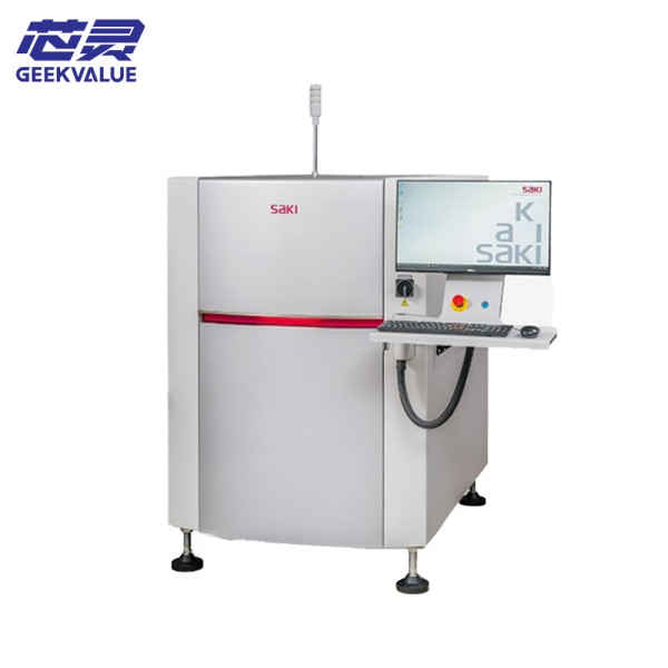
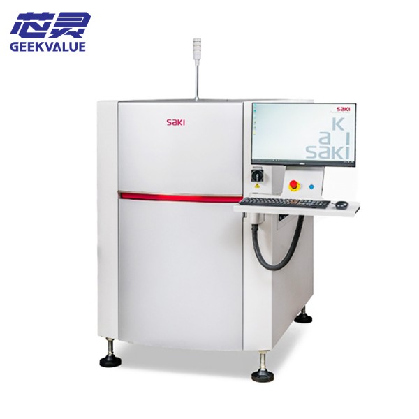
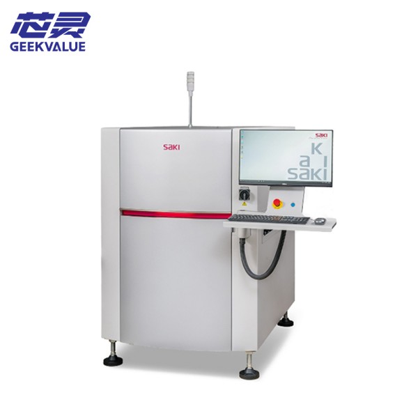
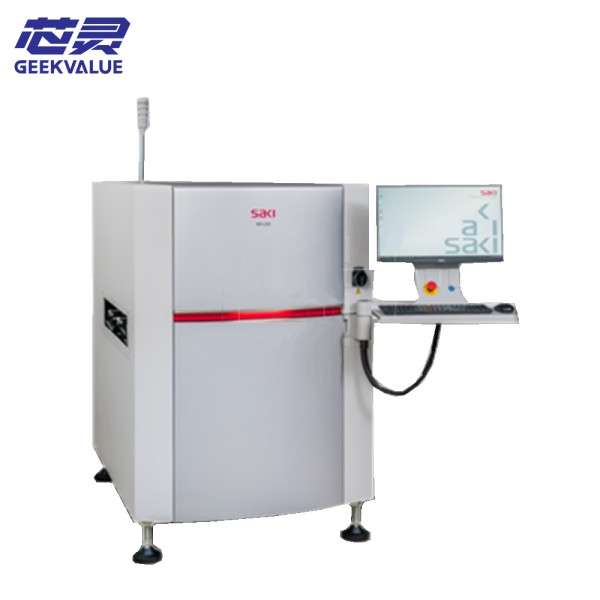
Model: SAKI BF-LU1
Type: High-speed 2D automatic optical inspection equipment (AOI)
Core positioning: PCB assembly rapid inspection for the middle and back end of SMT production lines (after reflow soldering), focusing on high cost performance and stable detection rate, suitable for cost-sensitive fields such as consumer electronics and industrial control.
Technical route: Pure 2D optical imaging, combined with multi-spectral lighting and algorithm optimization, balancing speed and accuracy.
2. Core technology and hardware configuration
(1) Optical imaging system
High-resolution camera:
Equipped with 5-megapixel to 20-megapixel CMOS camera (depending on the configuration), the minimum detectable component size is 01005 (0.4mm×0.2mm).
Multi-angle light source system:
Ring RGB + coaxial light combination, supports more than 16 lighting modes, enhances the contrast of solder joints, characters, and component bodies.
(2) Mechanical design
Modular structure:
Flexible selection of conveyor track width (supports board width 50mm~450mm) to adapt to multi-variety production.
High-speed motion control:
Adopting servo motor drive, the detection speed can reach 25cm²/s~40cm²/s (depending on complexity and configuration).
(3) Software function
SAKI standard detection algorithm:
Rule-based defect judgment, supports more than 50 defect types such as solder joints (insufficient tin, bridging), components (missing parts, offset, reverse polarity).
Simplified operation interface:
Graphical programming (Drag & Drop), supports offline recipe import, and line change time can be controlled within 15 minutes.
3. Core detection capabilities
(1) Solder joint detection
2D morphological analysis: judge solder paste anomalies (such as bridging, insufficient solder) by color, contour, area, etc.
Limitations: cannot directly measure solder joint height or volume, and has limited detection capabilities for BGA/CSP bottom solder joints.
(2) Component placement detection
Existence/polarity: identify 0402/0201/01005 components, IC direction, and mismatched parts (such as mixed resistors and capacitors).
Position accuracy: detect offset (±25μm), tilt (tombstone).
(3) Compatibility
Board type adaptation: rigid board, simple flexible board (special fixture required).
Component range: 01005 micro components to large electrolytic capacitors (height ≤15mm).
4. Typical application scenarios
Consumer electronics:
Home appliance control boards, LED lighting modules and other medium and low complexity PCBs.
Industrial control:
PLC modules, power management boards, which require detection speed over extreme accuracy.
Low-cost, high-volume production lines:
SMT workshops that need to quickly deploy AOI and have limited budgets.
5. Competitive advantages and limitations
(1) Advantages
Cost-effectiveness: significantly lower price than 3D AOI, simple maintenance (no laser module loss).
Speed priority: suitable for large-scale production lines, UPH (number of boards tested per hour) can reach 200~300 boards (depending on board size).
Ease of use: low operating threshold, suitable for technical workers to quickly get started.
(2) Limitations
2D technology limitations:
Unable to detect defects related to solder joint height (such as cold solder joints, coplanarity), and easy to misjudge highly reflective components (such as gold fingers).
Inapplicable scenarios:
Automotive electronics, medical equipment and other fields that have strict requirements for 3D quantitative detection.
6. Market Positioning Comparison
Comparison Items SAKI BF-LU1 (2D) SAKI 3Di Series (3D)
Detection Dimension 2D (plane) 3D (height + volume)
Solder Spot Detection Capability Depends on Color/Contour Directly Quantifies Tin Amount
Speed High Speed (25~40cm²/s) Medium-high speed (limited by 3D scanning)
Cost Low (about 1/3 of 3D AOI) High
Applicable Industries Consumer Electronics, Industrial Automobile, Medical, Semiconductor
7. User Selection Recommendations
Conditions for Selecting BF-LU1:
The production line is mainly based on medium and low complexity PCBs, and the budget is limited.
There is no rigid requirement for solder spot height detection, or the solder paste amount has been controlled by other means (such as SPI).
Situations Not Recommended:
BGA/QFN bottom solder joints or ultra-fine pitch components (<0.1mm) need to be detected.
8. Optional upgrade configuration
AI-assisted classification: Add AI module to reduce false alarms (additional license required).
Dual-track detection: Improve throughput (suitable for small-size boards).
9. Precautions
Environmental requirements: Avoid direct sunlight, and control temperature and humidity within the standard SMT workshop range (23±3°C, humidity <60%).