The following is a detailed introduction to SAKI 3D SPI 3Si-LS2
1. Equipment Overview
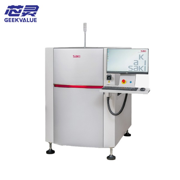
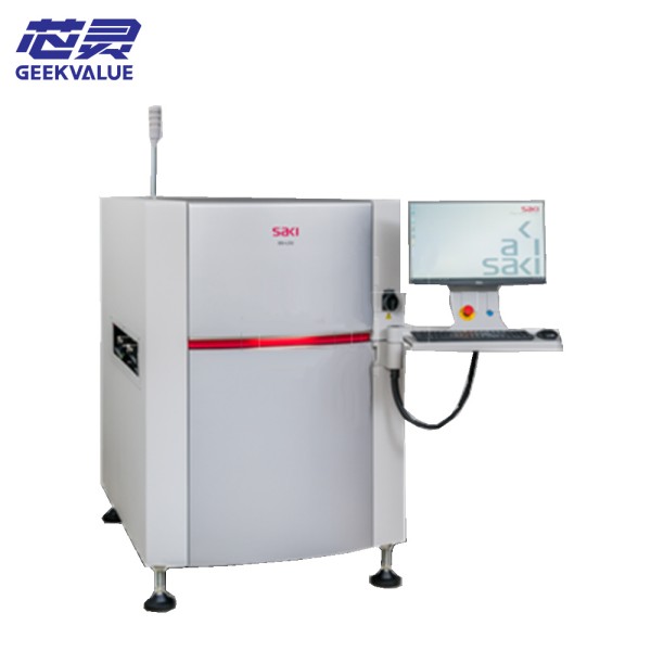
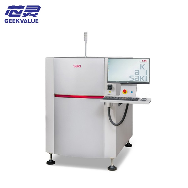
Model: SAKI 3Si-LS2
Type: 3D Solder Paste Inspector
Core Application: Used for SMT production line after printing and before patching to detect three-dimensional parameters such as solder paste volume, height, shape, etc., to ensure printing quality and prevent defects after reflow soldering.
Technical route: Use laser triangulation or structured light projection (depending on the configuration) to achieve high-precision 3D imaging.
2. Core Specifications
Item Parameter Details
Detection Technology Laser Scanning/Multi-frequency Structured Light (optional)
Z-axis resolution ≤1μm (repeatability)
Detection speed 15~50cm²/s (depending on accuracy requirements)
Minimum detection component 01005 (0.4mm×0.2mm)
Maximum board size 510mm×460mm (customizable)
Solder paste measurement parameters Volume, height, area, offset, bridging risk
3. Core technologies and functions
(1) High-precision 3D imaging
Laser triangulation:
Scan the solder paste surface with high-speed laser lines to generate 3D point cloud data to quantify the height, volume, and coplanarity of the solder paste.
The resolution can reach 0.5μm (Z-axis), which is suitable for ultra-fine pitch pads (such as 0.3mm pitch BGA).
Multi-spectral auxiliary lighting (optional):
Combined with RGB light source, it can simultaneously detect solder paste printing offset and steel mesh residue.
(2) Intelligent analysis software
SAKI SPI VisionPro:
Real-time SPC statistics: Generate solder paste height distribution map, Cpk/Ppk process capability index, and monitor printing process stability.
Defect warning: Automatically mark low tin, pull tip, and bridge risk areas, and compare with steel mesh design data.
AI adaptation: Learn the normal solder paste morphology of different pad types to reduce false alarm rate (<2%).
(3) Production line integration capability
MES/ERP interface: Support SECS/GEM protocol and upload inspection data in real time.
Closed-loop control: Link with solder paste printers (such as DEK, MPM) to automatically feedback and adjust scraper pressure or speed.
4. Core advantages
(1) Comparison with 2D SPI
Real volume measurement: Directly quantify the amount of solder paste to avoid 2D misjudgment caused by color or reflection.
Preventive control: Predict defects such as cold solder joints and tombstones after reflow soldering through height/volume analysis.
(2) Comparison with similar 3D SPI
Speed and accuracy balance: Laser scanning speed is better than moiré fringe projection SPI, suitable for high-speed production lines.
Adaptation to complex pads: Better detection effect on stepped steel mesh and micro-hole arrays (such as Flip Chip).
(3) Cost-effectiveness
Fast ROI: Reduce the defect rate after reflow by 30%~50%, reducing the cost of rework.
Low maintenance design: No vulnerable optical components (such as interferometers), high long-term stability.
5. Typical application scenarios
High-density electronics:
Smartphone motherboard (0.3mm pitch CSP), smart watch micro PCB.
Automotive electronics:
Engine control unit (ECU), ADAS sensor, requiring solder paste printing CPK ≥ 1.67.
Semiconductor packaging:
Wafer-level packaging (WLP) solder ball printing detection.
6. Common Errors and Solutions
Error Code Possible Cause Solution
ERR-LS-201 Laser calibration offset Execute the automatic calibration procedure or manually adjust the optical path.
ERR-MOT-305 Motion platform out of limit Check whether the PCB clamp is in place and reset the motion module.
ERR-CAM-412 Camera image is blurred Clean the lens, check the focus motor or recalibrate.
WARN-DATA-503 Detection data overflow (abnormally high solder paste) Confirm whether the steel mesh cleanliness or printer parameters are abnormal.
7. Maintenance and calibration
Daily maintenance:
Clean the laser window and glass table daily to prevent dust from affecting the imaging.
Regular calibration:
Verify the Z-axis accuracy using a standard calibration plate (with a known height step) every month.
Life of key components:
The laser module life is about 20,000 hours, and the power attenuation needs to be monitored.
8. Market positioning comparison
Comparison items SAKI 3Si-LS2 Competitors (such as Koh Young KY8030)
Detection technology Laser scanning Moiré fringe projection
Z-axis resolution 0.5μm 0.3μm (higher cost)
Speed High speed (30cm²/s@10μm) Medium speed (20cm²/s@5μm)
AI function Built-in adaptive algorithm Additional authorization required
Price Mid-to-high-end (outstanding cost-effectiveness) High-end (premium 20%~30%)
9. User selection suggestions
Recommended selection scenarios:
Production lines have strict requirements on solder paste volume consistency (such as automotive electronics).
High-mix production needs to respond quickly (frequent line changes).
")