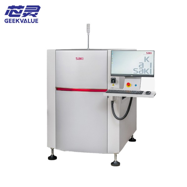
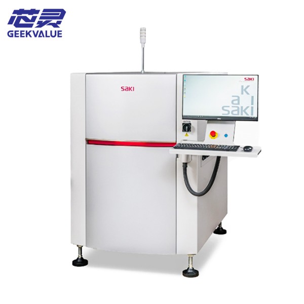
The following is a detailed introduction to SAKI 3D AOI 3Di-LS3EX
1. Equipment Overview
Model: SAKI 3Di-LS3EX
Type: High-precision 3D automatic optical inspection equipment (AOI)
Core positioning: Quality inspection for high-density PCB assembly (SMT) and complex packaging processes, especially good at three-dimensional quantitative analysis of tiny solder joints and hidden defects.
Technical route: Combining laser scanning 3D imaging with multi-spectral 2D detection to achieve full-view coverage.
2. Core technology and hardware configuration
(1) 3D imaging system
Laser triangulation technology:
Through high-speed laser line scanning, the height, volume, coplanarity and other three-dimensional data of solder joints are obtained, and the Z-axis repeatability can reach ±1μm.
Supports multi-angle synchronous scanning to eliminate shadow blind areas (such as BGA bottom solder balls).
Multi-spectral 2D auxiliary imaging:
Equipped with RGB+infrared light source to enhance the 2D recognition ability of component markings and polarity characters.
(2) High-speed and high-precision motion system
Linear motor drive:
Scanning speed can reach 500mm/s~1m/s (depending on the configuration), suitable for high-speed SMT production lines (UPH≥400 boards).
Adaptive focus:
Automatically compensate for PCB warpage or tray thickness differences to ensure imaging consistency.
(3) Intelligent software platform
SAKI VisionPro or AIx platform (depending on the version):
Defect classification AI: Automatically learn abnormal solder joint patterns (such as voids, cracks), with a false alarm rate (False Call) less than 1%.
SPC data analysis: Real-time generation of solder paste height distribution map and defect Pareto chart to support process optimization.
3. Core detection capabilities
(1) 3D solder joint detection
Quantitative parameters: solder joint height, volume, contact angle, coplanarity.
Typical defects:
Hot solder joint, insufficient solder, bridging, solder ball, tombstoning effect.
BGA/CSP/QFN hidden solder joint detection (through edge laser penetration scanning).
(2) Component placement detection
Presence/polarity: Identify 0201/01005 micro components, IC direction, and misaligned components.
Position accuracy: Detect offset (±15μm), tilt (such as connector warping).
(3) Compatibility
Board type: rigid board, flexible board (FPC), substrate with bumps (such as flip chip).
Component range: 01005 micro components to large heat dissipation modules (maximum board size depends on configuration, typical value 610mm×510mm).
4. Industry application scenarios
High-end consumer electronics:
Smartphone motherboard (POP packaging), TWS headset micro PCB.
Automotive electronics:
ADAS module, car camera module (compliant with AEC-Q100 reliability standards).
Semiconductor packaging:
SiP (system-level packaging), Fan-Out wafer-level packaging appearance inspection.
5. Competitive advantages
(1) Comparison with 2D AOI
Three-dimensional quantification: Directly measure the amount of solder to avoid 2D color/shadow misjudgment.
Complex component coverage: has obvious advantages in bottom terminal components (BTC) and solder joints under shielding covers.
(2) Comparison with similar 3D AOI
Speed and accuracy balance: Laser scanning speed is better than structured light projection 3D AOI.
Data fusion: 3D+2D hybrid detection, taking into account height data and surface features (such as character recognition).
(3) Production line integration
MES/ERP interface: Supports SECS/GEM protocol to achieve real-time upload of detection data.
Linkage with SPI: Predict solder joint defect risks through solder paste printing data.
6. Optional expansion functions
Dual-track detection module: Parallel detection of dual boards, increasing production capacity by more than 30%.
AI self-learning: Dynamically update the defect library to adapt to the rapid introduction of new products.
3D modeling simulation: Offline simulation of the detection process, and optimization of the detection path in advance.
7. User pain point solution
Problem: Low efficiency of manual re-inspection after micro-component (01005) mounting.
→ 3Di-LS3EX solution: 3D+2D composite inspection, automatic defect classification, and re-inspection rate reduced to less than 5%.
Problem: Strict reliability requirements for automotive PCB solder joints (such as no voids).
→ Solution: 100% full inspection through quantitative analysis of solder joint volume/void rate.
8. Notes
Verification requirements: It is recommended to provide actual product sample testing for the minimum detectable defect size (such as 0.1mm² of insufficient tin).
Maintenance cost: The laser module has a life of about 20,000 hours and needs to be calibrated regularly.
")