ave up to 70% on SMT Parts – In Stock & Ready to Ship
Get Quote →The ASM AD838 die bonder is a precision semiconductor backend equipment platform designed for stable, high-yield die attach processes in advanced electronics manufacturing. It is widely deployed in production environments requiring consistent bonding accuracy and long-term process stability.
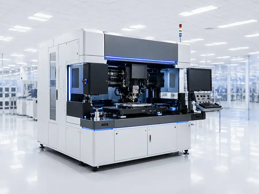
The ASM AD838 die bonder is a semiconductor backend die attach machine used for precise bonding of silicon dies onto substrates during IC packaging processes. It is designed for stable, high-precision operation in automated semiconductor production environments.
As a core type of die bonding machine, the AD838 performs controlled die placement using optical alignment, motion control systems, and regulated bonding force. It is widely used in IC assembly, LED packaging, and power semiconductor manufacturing.
ASM AD838 functions as a precision die attach system in semiconductor backend manufacturing, ensuring accurate placement and reliable bonding of micro-scale chips.
The ASM AD838 die bonder is built on a multi-layer semiconductor automation architecture. Each subsystem works together to ensure precision die placement, stable bonding force control, and high-yield production performance.
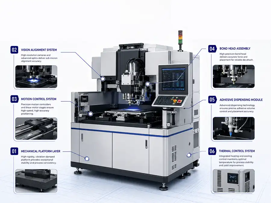
Provides the structural base of the ASM AD838 system, ensuring vibration stability and mechanical precision during high-speed operations.
High-resolution optical inspection module for die recognition, alignment correction, and positional accuracy control before bonding.
Multi-axis precision motion control responsible for die pickup, placement trajectory, and micro-positioning accuracy.
Core execution unit that performs die attach operations with controlled force, speed, and placement accuracy.
Controls epoxy or solder dispensing with micro-volume accuracy to ensure consistent bonding layer thickness.
Maintains stable temperature conditions during bonding and curing processes to ensure long-term reliability.
The ASM AD838 architecture integrates mechanical stability, optical alignment, and motion precision into a unified die bonding system, enabling consistent semiconductor packaging performance in high-volume production environments.
The ASM AD838 die bonder executes a fully automated die attach workflow designed for high-precision semiconductor packaging. Each stage is optimized for alignment accuracy, placement stability, and thermal bonding reliability.
Vacuum collet precisely picks individual dies from wafer or tray with controlled force to prevent damage.
High-resolution optical system identifies die orientation and corrects positional deviation before placement.
Controlled epoxy or solder dispensing ensures uniform bonding layer thickness for stable adhesion.
The AD838 bonding head performs high-speed, sub-micron placement of the die onto substrate with precise force control.
Heat and pressure are applied to ensure mechanical and electrical stability of the die attachment.
Final curing process solidifies adhesive and ensures long-term reliability under thermal cycling conditions.
| Parameter | Value |
|---|---|
| Equipment Type | Die Bonding Machine |
| Process | Die Attach / Epoxy / Solder |
| Precision | Sub-micron alignment capability |
| Applications | IC / LED / Power Semiconductors |
| Platform | ASM AD Series |
The ASM AD838 die bonding machine is used across multiple semiconductor backend manufacturing industries where high precision die attach processes are required.
Used in integrated circuit assembly lines for precise die placement on substrates with high yield stability.
Supports MOSFET, IGBT, and power module packaging requiring strong thermal and mechanical bonding.
High-volume die attach for LED chips with consistent brightness and thermal performance control.
Used in ECU, ADAS, and sensor module production requiring high reliability and long lifecycle stability.
Applied in RF front-end modules and communication IC packaging requiring precision alignment.
Supports heterogeneous integration and high-density packaging processes in modern semiconductor fabs.
In semiconductor backend packaging, ASM AD838, BESI die bonders, and K&S (Kulicke & Soffa) systems are widely used in different production scenarios. The comparison below highlights differences in precision, application focus, and production positioning.
Position: High-precision mainstream production system
Strength: Stable die attach, strong process control, high yield consistency
Best for: IC packaging, LED, power devices, automotive electronics
Keyword: ASM AD838 die bonder / ASM die bonding machine
Position: Advanced packaging & high-end flip chip systems
Strength: Extremely high precision, advanced hybrid bonding capability
Best for: Advanced packaging, wafer-level integration, high-end semiconductor fabs
Note: Higher cost, focused on cutting-edge process nodes
Position: Flexible wire bonding & die attach platform
Strength: Versatile, widely used in mid-range semiconductor production
Best for: General IC assembly, legacy production lines, cost-sensitive fabs
Note: Strong installed base, but lower automation level vs newer systems
If the requirement is stable high-volume die attach production, ASM AD838 remains a strong balanced solution. BESI is preferred for advanced packaging innovation, while K&S systems are often used in cost-efficient or legacy production environments.
It is used for semiconductor die attach processes in IC packaging, LED assembly, and power semiconductor manufacturing.
Yes, it is a high-precision die bonding machine designed for automated chip placement onto semiconductor substrates.
A die bonder attaches silicon chips to substrates, while a wire bonder connects electrical terminals using fine wires.
It is widely used in semiconductor packaging, automotive electronics, LED manufacturing, and power device production.
Yes, it is designed for stable high-yield production environments requiring consistent die placement accuracy.
It supports epoxy bonding, solder bonding, and adhesive die attach processes depending on application requirements.
It is engineered for sub-micron level alignment accuracy in advanced semiconductor packaging processes.
Yes, it is widely used in secondary markets, refurbished semiconductor equipment lines, and legacy production systems.
Why do so many people choose to work with GeekValue?
Our brand is spreading from city to city, and countless people have asked me, "What is GeekValue?" It stems from a simple vision: to empower Chinese innovation with cutting-edge technology. This is a brand spirit of continuous improvement, hidden in our relentless pursuit of detail and the delight of exceeding expectations with every delivery. This almost obsessive craftsmanship and dedication is not only the persistence of our founders, but also the essence and warmth of our brand. We hope you will start here and give us an opportunity to create perfection. Let us work together to create the next "zero defect" miracle.
DetailsContact a sales expert
Reach out to our sales team to explore customized solutions that perfectly meet your business needs and address any questions you may have.

© All Rights Reserved. Technical Support:TiaoQingCMS