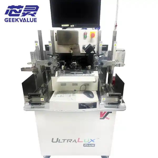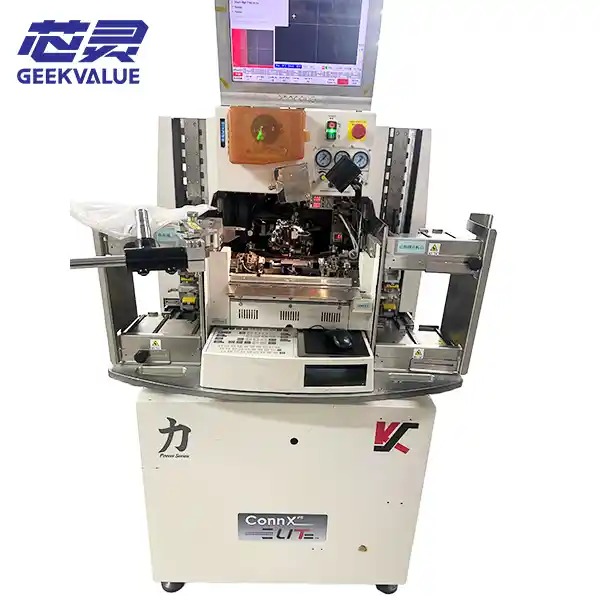
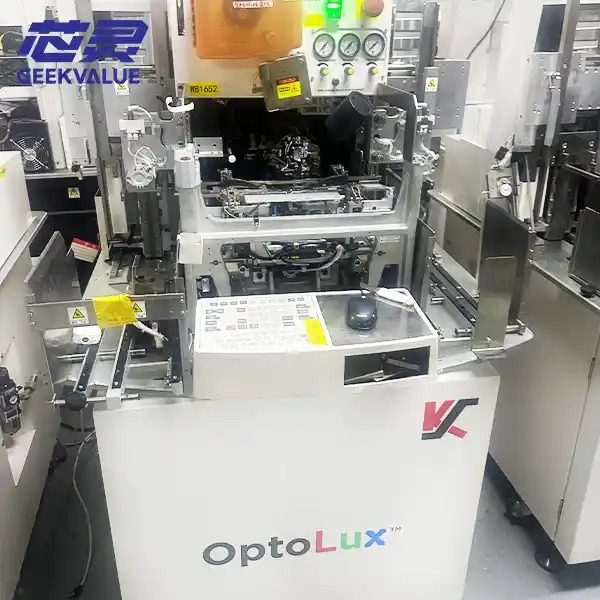
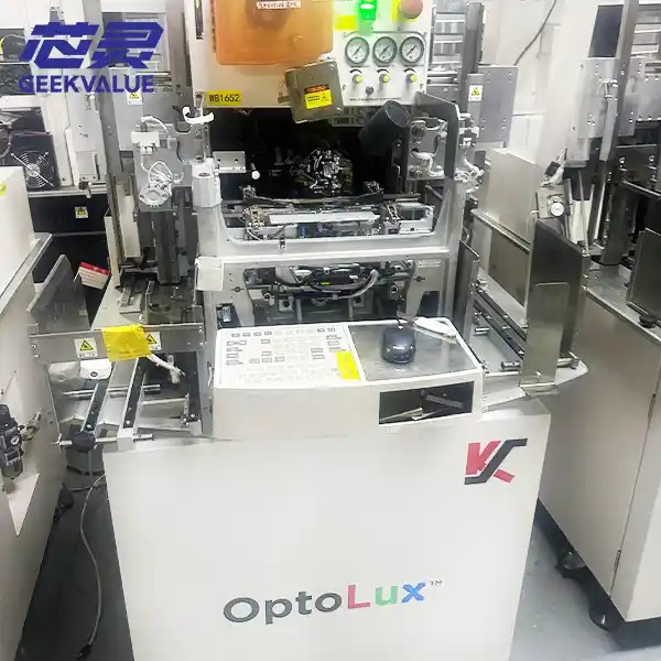
 OptoLux™ is a fully automated ultrasonic ball bonding machine from K&S (Kulisofa) for LED optoelectronic packaging. It's a classic platform for large-scale production of LEDs and optoelectronic devices, later upgraded to the OptoLux™ Plus version. The equipment focuses on lighting LEDs, Mini-LEDs, and infrared optoelectronic devices, balancing capacity, bonding yield, and process compatibility, and is widely used in optoelectronic packaging production lines worldwide.
I. Equipment Positioning
OptoLux™ is positioned as a medium-to-high-speed dedicated ball bonder for optoelectronics, focusing on interconnecting discrete optoelectronic devices, completing ultrasonic ball bonding of gold wire, silver alloy, and copper wire between chip pads and the substrate/support. It is suitable for high-volume production of SMD LEDs, high-power LEDs, infrared emitters and receivers, and optoelectronic sensors; while also considering ease of debugging, it is suitable for small to large LED packaging plants, but not for high-end logic IC chip packaging.
II. Core Hardware System
X-Y-Z High-Speed Servo Motion Platform: Closed-loop servo drive optimizes the motion trajectory of the continuous support structure, reduces idle travel loss, and ensures basic UPH production capacity; high-precision Z-axis pressure closed-loop control reduces the risk of damaging the chip PAD for thin LED electrodes.
Programmable Look-Ahead Vision System: Pre-scanning and pre-judging positioning shortens image acquisition waiting time; equipped with a WAVI wide-angle vertical illumination system, red and blue programmable light sources + low-angle oblique illumination, to cope with reflections from electroplated supports and interference from color differences in the supports, improving PRS positioning stability.
Built-in SHTL and NSOL automatic fault recovery logic automatically retry when anomalies are identified, reducing downtime and improving the average auxiliary interval time of MTBA.
Optical System: Standard 2× magnification optics, accommodating both large field-of-view scanning and pad observation, meeting the needs of conventional LED and early Mini-LED pad identification.
Quick-LED Suite LED-Specific Process Kit
K&S offers a customized process database for optoelectronic packaging, incorporating mature wire arc, ignition, and ultrasonic-pressure timing parameters. Combined with ACCUBMP solder ball guiding technology, it ensures solder ball consistency, enabling rapid commissioning of new machines and lowering the barrier to process setup.
Equipped with the Auto-BITS self-optimization algorithm, it automatically learns and dynamically corrects bonding parameters during equipment operation, compensating for process drift caused by cleaver wear and wire material fluctuations, thus stabilizing batch yield.
III. Key Process Specifications
Compatible Wires: Gold wire, silver alloy wire, palladium-copper wire; optional microenvironment protection kit supports copper wire production and suppresses copper wire arcing and oxidation.
Applicable Wire Diameter: 20-50μm, covering mainstream wire diameters for conventional lighting and high-power LEDs.
Bonding Accuracy: ±3μm@3σ, meeting the bonding requirements of small and medium pads.
Effective Bonding Processing Area: 56×80mm, compatible with conventional LED cascade supports and ceramic substrates.
Wire Arc Capability: Supports low arc, standard arc, and high arc, compatible with supports of different cavity depths.
Feeding Compatibility: Supports trays and cascade supports; can be integrated with automated loading and unloading systems; supports MES data traceability.
IV. Main Application Areas
LED Packaging: 2835, 3030, 5050 and other SMD surface mount LEDs, high-power ceramic LEDs, COB chips, early Mini-LED mass production wire bonding.
Optoelectronic Devices: Infrared IR emitting/receiving tubes, photoelectric sensors, optocoupler discrete devices.
Consumer Optoelectronic Device Discrete Device Packaging
V. Core Advantages of the Equipment
Deep Adaptation to Optoelectronic Processes: Specifically optimized to address pain points such as reflectivity in LED electroplating brackets and susceptibility to pressure damage from thin electrodes, resulting in a wide process window and stable mass production yield.
Low Learning Curve: The Quick-LED Suite pre-packaged process allows for short setup times when switching to new models, reducing reliance on senior process engineers.
Excellent Operational Performance: Visual automatic fault recovery + Auto-BITS adaptive compensation minimizes downtime due to human intervention, making it suitable for long-term, uninterrupted mass production.
Expandable Wire Supply: On-site upgrades to a microenvironment kit allow for switching from gold wire production lines to silver alloy or copper wire, supporting cost reduction solutions for factories.
Convenient Maintenance: Modular design allows for easy assembly and disassembly of the splitter, firing pin, and wire feeding mechanism, reducing maintenance time.
VI. Brief Differences Between OptoLux™ and OptoLux™ Plus
OptoLux™ (Basic Version): A classic LED mass production platform, mature and stable, meeting the production capacity needs of conventional SMD and high-power LEDs, geared towards standard LED mass production.
OptoLux™ Plus (Upgraded Version): Features upgraded servo motion, iterated vision algorithms, further improved UPH (Upgraded Per Hour), and enhanced robustness for copper wire bonding and Mini-LED small pad processes, making it suitable for high-volume production lines with higher requirements.
VII. Summary K&S OptoLux™ is a benchmark ball bonding equipment in the LED packaging industry. Its core features are maturity, stability, process-friendly operation, and simple maintenance. It effectively solves the pain points of traditional LED bracket reflection, solder ball inconsistency, and long-term process drift during production; it is the mainstream choice for traditional lighting LED and infrared optoelectronic device production lines.