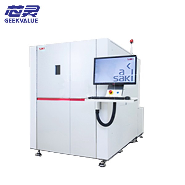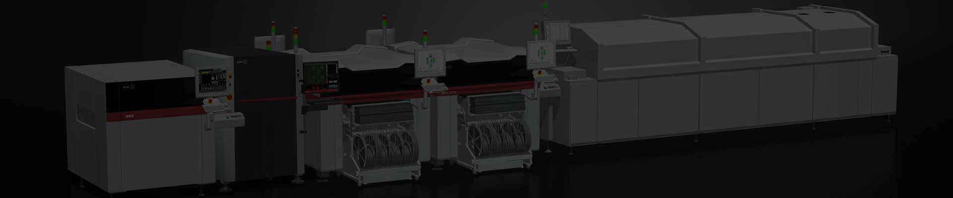
In the modern electronics manufacturing industry, the inspection requirements for PCB (printed circuit boards) are getting higher and higher, especially the welding quality inspection of high-density packages (such as BGA, QFN, CSP) and micro components (such as 0201, 01005). Traditional 2D AOI (automatic optical inspection) equipment has been difficult to meet high-precision requirements, and SAKI 3Di-LS3 3D AOI provides a more accurate and efficient inspection solution for SMT (surface mount technology) production lines with its advanced 3D imaging technology and intelligent algorithms.
Product advantages
✅ High-precision 3D inspection: Using laser scanning technology, key parameters such as solder joint height, coplanarity, and volume can be accurately measured to reduce misjudgment.
✅ High-speed inspection: Optimizing the optical system and algorithm, the inspection speed is more than 20% higher than that of traditional 3D AOI, which is suitable for high-speed SMT production lines.
✅ Intelligent defect recognition: AI algorithm automatically learns and optimizes to reduce false alarm rate (False Call) and improve inspection reliability.
✅ Wide compatibility: supports all types of PCB board types (rigid, flexible, HDI) and complex components (BGA, LGA, PoP, etc.).
✅ Modular design: detection functions can be expanded according to customer needs, such as SPI (solder paste detection) linkage to achieve closed-loop process control.
Working principle
SAKI 3Di-LS3 uses laser triangulation technology, combined with a high-resolution CCD camera, to achieve 3D imaging:
Laser scanning: The laser line is projected onto the PCB surface, and the camera captures the reflected light from different angles to calculate the solder joint height data.
3D modeling: Through multi-angle scanning, the 3D profile of the solder joint is generated, and the height, volume, shape and other parameters are accurately measured.
AI analysis: The algorithm based on deep learning automatically compares the standard solder joint model to identify defects such as cold solder joints, insufficient solder, bridging, and offset.
Core functions
1. 3D solder joint detection
Measure the height, volume, and coplanarity of the solder joint to ensure the soldering quality of hidden solder joints such as BGA and QFN.
Detect common defects such as insufficient solder paste, solder balls, and tombstoning.
2. High-precision component detection
Identify problems such as placement offset, tombstone, and rollover of ultra-small components such as 0201 and 01005.
Support 3D contour detection of special-shaped components, shielding covers, and connectors.
3. Intelligent data analysis
Automatically generate SPC (statistical process control) reports to optimize production processes.
Integrate with MES (manufacturing execution system) to achieve data traceability and real-time monitoring.
4. Flexible programming and debugging
Provide a graphical programming interface, support offline programming (OLP), and shorten line change time.
Auto-learning function to reduce manual debugging workload.
Product features
📌 Optical system
High-resolution laser scanning: accuracy can reach ±1μm, suitable for ultra-fine pitch component detection.
Multi-angle light source: ring LED + coaxial light combination to eliminate shadow interference and improve imaging quality.
📌 Software Algorithm
AI Deep Learning: Automatically optimizes detection parameters to adapt to different PCB designs.
Adaptive Threshold: Reduces misjudgments caused by PCB color, reflections, etc.
📌 Mechanical Structure
High Rigidity Frame: Reduces vibration impact and ensures scanning stability.
Autofocus System: Adapts to different board thicknesses without manual adjustment.
Technical Specifications
Project Parameters
Detection accuracy ±1μm (Z axis)
Detection speed Up to 25cm²/s
Minimum component size 01005 (0.4mm × 0.2mm)
Laser wavelength 650nm (red laser)
Camera resolution 12MP (4096×3072)
Compatible PCB size 50mm × 50mm ~ 510mm × 460mm
Communication interface SECS/GEM, TCP/IP
Power requirement AC 200-240V, 50/60Hz
Application scenarios
Consumer electronics: High-density PCB detection of mobile phones, tablets, and smart wearable devices.
Automotive electronics: Welding quality control of key components such as ADAS and ECU.
Industrial control: PCB reliability detection of servers and communication base stations.
Conclusion
SAKI 3Di-LS3 3D AOI has become an indispensable quality control equipment in modern electronic manufacturing with its high-precision laser scanning, AI intelligent algorithm and high-speed detection capabilities. Whether dealing with miniaturized components or complex packaging processes, it can provide more reliable and efficient detection solutions to help customers improve yield and reduce production costs.
")