 EN
EN id
id sk
sk sr
sr sv
sv it
it pt
pt bn
bn ms
ms be
be nl
nl fr
fr th
th vi
vi ru
ru ja
ja ko
ko de
de hy
hy az
az bs
bs bg
bg my
my cs
cs da
da dv
dv el
el et
et fil
fil fi
fi ga
ga gl
gl gn
gn he
he hi
hi km
km hr
hr hu
hu is
is kn
kn rw
rw lo
lo lv
lv lt
lt lb
lb lg
lg mi
mi mt
mt ne
ne no
no ny
ny or
or om
om per
per pl
pl ro
ro sa
sa so
so es
es sw
sw ta
ta tr
tr uk
uk ur
ur cy
cy xh
xh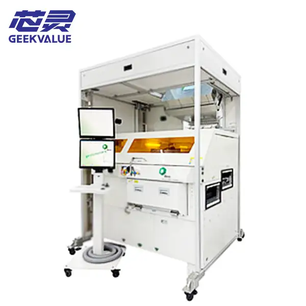
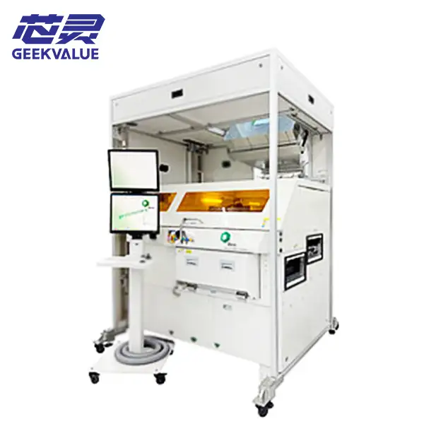 The Besi Datacon 8800 CHAMEO ultra plus AC is the flagship product of BE Semiconductor Industries (Besi)—the undisputed global leader in the hybrid bonding market. With its astonishing precision of up to 100 nm and a balanced throughput of 2,000 CPH, it has established itself as a pivotal player in the current revolution in AI and High-Performance Computing (HPC). It serves as the core driving force propelling hybrid bonding technology from the laboratory into large-scale mass production.
**Market Position: A Near-Monopolistic Industry Leader**
Besi holds a dominant position in the global hybrid bonding equipment market; specifically within the critical Die-to-Wafer hybrid bonding segment, it commands a market share of approximately 91%. This standing has led market research firms to regard Besi as the "most promising technological leader" in this field since ASML’s introduction of EUV lithography.
**Core Technology: The "Secret Sauce" for Achieving Nanoscale Bonding**
The exceptional performance of Besi’s flagship model—the Datacon 8800 CHAMEO ultra plus AC—is powered by a comprehensive and sophisticated technological system:
**Extreme Precision and High-Quality Output:** Built upon the proven Datacon platform, this equipment performs direct fusion bonding of dielectric layers at room temperature, followed by batch annealing to complete the electrical interconnections.
**Rigorous Cleanliness Management:** Hybrid bonding is extremely sensitive to particulate contamination. The equipment's working area provides an ISO Class 3 cleanroom environment—far exceeding the capabilities of most comparable systems on the market—thereby maximizing bonding yield.
**Sub-Micron Interconnection Capability:** It achieves ultra-high alignment accuracy of 200 nanometers and interconnection pitches as fine as 1 micron. This capability is critical for realizing ultra-fine-pitch copper-to-copper direct interconnections, significantly boosting both interconnection density and energy efficiency.
**Comprehensive Process Compatibility:** The equipment supports a wide range of processes, including Fan-Out Wafer-Level Packaging (FO-WLP), Advanced Chip-to-Wafer bonding, and Through-Silicon Via (TSV)-related processes. Furthermore, it employs technologies such as "Van Gogh" high-precision optical alignment and "Van Gogh" Inline IR inspection to facilitate process control and yield enhancement.
Material and Handling Capabilities: The equipment is capable of processing ultra-thin chips with a thickness of merely 25 microns (μm). It also supports various ejection schemes—including standard pin-type, multi-stage, and UV-assisted methods—to accommodate different types of chips.
Automation and Integration: Equipped with Full Factory Automation capabilities, the system can execute fully automated material changeovers triggered directly by a host system. Moreover, it integrates deeply with equipment from Applied Materials to form a complete, end-to-end solution, thereby maximizing the efficiency of the interplay between front-end and back-end processes.
Application Areas: The "Engine" for AI and Advanced Packaging
The equipment's key application scenarios primarily span the heterogeneous integration of AI/HPC chipsets, High Bandwidth Memory (HBM) manufacturing, as well as 3D NAND and CIS (CMOS Image Sensor) technologies; it serves as a core piece of equipment underpinning today's cutting-edge technology products.
Ecosystem and Partnerships
Besi pursues two key strategies to drive the development of the industry ecosystem:
Strategic Alliances: Besi has established a deep strategic partnership with Applied Materials, through which the two companies jointly developed and launched "Kinex"—an integrated D2W (Die-to-Wafer) hybrid bonding system. Additionally, Applied Materials holds approximately 9% of Besi's shares, making it Besi's largest shareholder and providing substantial financial and technical support.
Customer Validation: NHanced Semiconductors—a specialized advanced packaging foundry—was the first company globally to introduce this platform into commercial production. The platform enabled a nearly tenfold increase in throughput.
Market Performance and Strategic Direction
Besi is clearly advancing toward higher precision and larger market segments:
Robust Financial Performance: In the first quarter of 2026, the company's order intake reached €269.7 million—a year-over-year surge of 104.5%—demonstrating the strong demand driven by AI applications. Furthermore, the gross margin for its advanced packaging business has remained stable at approximately 63.5%. A Continuously Advancing Technological Roadmap: Besi is already planning next-generation equipment capable of achieving precision levels as high as 50 nanometers (nm) to address the challenges of future, more advanced chip integration, thereby fortifying its technological barriers.
A Continuously Advancing Technological Roadmap: Besi is already planning next-generation equipment capable of achieving precision levels as high as 50 nanometers (nm) to address the challenges of future, more advanced chip integration, thereby fortifying its technological barriers.
Industry Assessment and Future Outlook
Backed by its clear technological and commercial prospects, Besi is regarded by the market as the European semiconductor equipment company poised for the strongest growth over the coming years. Analysts project that its earnings per share could quadruple within four years. The Datacon 8800 CHAMEO ultra plus AC serves as the very cornerstone supporting this ambitious vision. Acting as a bridge connecting AI computing power with the physical world, Besi stands at the epicenter of a structural industry trend—the semiconductor sector's evolution toward advanced packaging and heterogeneous integration.