 EN
EN id
id sk
sk sr
sr sv
sv it
it pt
pt bn
bn ms
ms be
be nl
nl fr
fr th
th vi
vi ru
ru ja
ja ko
ko de
de hy
hy az
az bs
bs bg
bg my
my cs
cs da
da dv
dv el
el et
et fil
fil fi
fi ga
ga gl
gl gn
gn he
he hi
hi km
km hr
hr hu
hu is
is kn
kn rw
rw lo
lo lv
lv lt
lt lb
lb lg
lg mi
mi mt
mt ne
ne no
no ny
ny or
or om
om per
per pl
pl ro
ro sa
sa so
so es
es sw
sw ta
ta tr
tr uk
uk ur
ur cy
cy xh
xh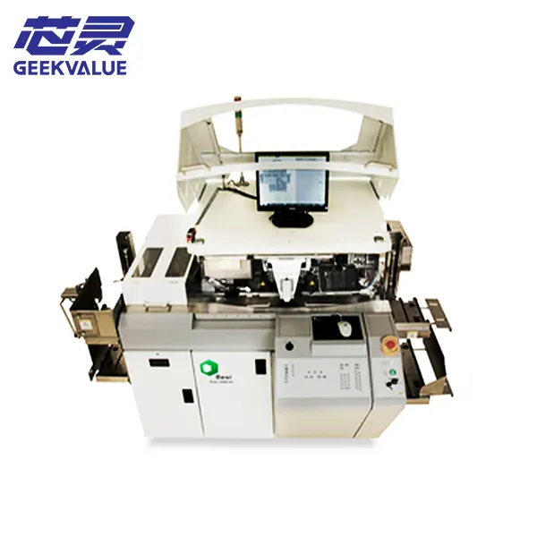
Part of the BESI Die Bonder Family
The ESEC 2100 hS belongs to the industry-leading BESI Die Bonder product portfolio, a range of semiconductor die attach platforms recognized worldwide for their reliability, throughput, and long-term production stability.
Other popular BESI die bonding solutions include the Datacon 8800 FC QUANTUM for high-speed flip chip assembly and the Datacon 8800 CHAMEO for advanced packaging applications.
Proven High-Speed Die Bonder for High-Volume Semiconductor Packaging
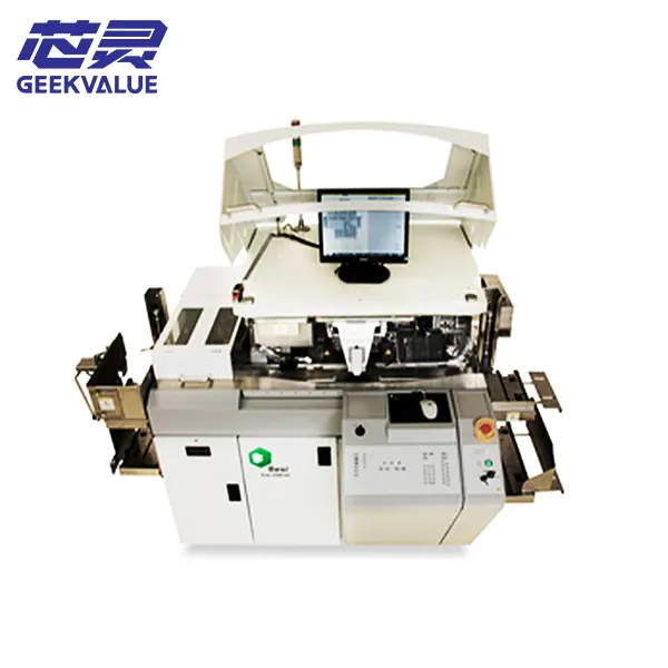
The BESI ESEC 2100 hS is one of the most widely deployed high-speed die bonders in semiconductor packaging facilities worldwide. Designed for maximum throughput, stable operation, and low cost of ownership, it remains a preferred platform for OSATs, IDMs, and semiconductor manufacturers producing millions of packages every month.
Combining exceptional speed, proven reliability, and flexible process capability, the ESEC 2100 hS has become a benchmark solution for epoxy die attach applications across automotive electronics, power semiconductors, industrial devices, memory products, sensors, and consumer electronics.
Whether you are expanding production capacity, replacing legacy equipment, or seeking a cost-effective refurbished die bonder, the ESEC 2100 hS remains one of the most trusted production platforms available today.
Why Choose the ESEC 2100 hS?
Proven in Semiconductor Manufacturing Worldwide
The ESEC 2100 hS has been successfully deployed in semiconductor assembly plants around the world for years. Its mature platform design has been validated through millions of production hours, making it one of the safest investments for semiconductor packaging operations.
Exceptional Throughput
With production speeds reaching up to 18,500 UPH, the ESEC 2100 hS delivers outstanding productivity for high-volume manufacturing environments.
Its innovative Phi-Y motion concept significantly reduces travel time between pick and place operations, maximizing machine utilization and output.
Excellent Cost of Ownership
High throughput, rapid product changeover, long-term reliability, and modular upgrade options combine to deliver one of the industry's lowest cost-per-unit production solutions.
Easy Spare Parts and Engineering Support
Because of its large installed base worldwide, spare parts, tooling, vision systems, bond heads, and technical support remain readily available, helping manufacturers minimize downtime and extend equipment life.
Typical Applications
The ESEC 2100 hS supports a wide range of mainstream semiconductor packaging applications.
Power Semiconductor Devices
MOSFET
IGBT
Power Modules
Power Management ICs
Automotive Electronics
Automotive MCU
Driver IC
Automotive Sensors
Power Control Modules
Consumer Electronics
Memory Devices
RF Components
LED Drivers
Communication ICs
Industrial Electronics
Analog Devices
Industrial Controllers
Smart Sensors
Industrial Power Modules
For manufacturers expanding beyond conventional die attach processes, our Flip Chip Bonder solutions provide advanced packaging capability and higher interconnect density for next-generation semiconductor products.
Many semiconductor assembly lines also operate Wire Bonder systems alongside die bonding equipment, making process compatibility and production stability critical factors when selecting equipment.
As part of our complete BESI Die Bonder portfolio, the ESEC 2100 hS remains one of the most proven and reliable high-volume packaging platforms available today.
Semiconductor Assembly Process Integration
The ESEC 2100 hS is commonly deployed as part of a complete semiconductor assembly line. After die attach, devices typically move to subsequent packaging processes such as wire bonding, molding, singulation, and final testing.
For traditional semiconductor packaging, manufacturers often combine the ESEC 2100 hS with high-performance Wire Bonder systems to create stable and cost-effective production lines capable of handling large-volume manufacturing requirements.
Core Technology
Phi-Y Motion Concept
The ESEC 2100 hS utilizes BESI's proprietary Phi-Y motion architecture.
Unlike traditional die bonders relying purely on linear movement, the Phi-Y system combines rotational and linear motion to significantly reduce idle travel time and improve production efficiency.
Light & Rigid Pick-and-Place Structure
The machine's lightweight yet highly rigid pick-and-place structure enables exceptional dynamic stability during high-speed operation.
This design ensures precise placement performance while maintaining maximum throughput.
Advanced Motion Controller
Enhanced motion trajectory optimization minimizes vibration and ensures smooth die placement even at peak operating speeds.
Modular Substrate Handler Platform
Flexible substrate handling options allow manufacturers to configure the system for various package types and production requirements.
Key Features
Ultra-High Throughput
Up to 18,500 UPH
120 ms cycle time
Optimized for high-volume production
High Placement Accuracy
Standard Accuracy: 20 μm @ 3 Sigma
High Accuracy Mode: 15 μm @ 3 Sigma
Flexible Process Capability
Supports:
Epoxy Die Attach
Eutectic Bonding
Thermocompression Bonding
Reflow Soldering
High-Resolution Vision System
Optional high-resolution vision systems improve die alignment and placement accuracy for demanding applications.
Dual Dispensing Module
Dual independent dispensing axes increase throughput while maintaining process consistency.
Real-Time Process Monitoring
Operators can monitor:
Wafer status
Leadframe status
Strip status
Hopper status
Production performance
in real time.
Technical Specifications
| Specification | Details |
|---|---|
| Equipment Model | ESEC 2100 hS |
| Equipment Type | Fully Automatic High-Speed Die Bonder |
| Maximum Throughput | Up to 18,500 UPH |
| Cycle Time | 120 ms |
| Standard Accuracy | 20 μm @ 3 Sigma |
| High Accuracy Mode | 15 μm @ 3 Sigma |
| Die Size Range | 0.25 mm – 20 mm |
| Die Thickness | >0.075 mm |
| Wafer Size | 4" – 12" |
| Bond Force | 0.2 N – 20 N |
| Leadframe Length | 90 – 300 mm |
| Leadframe Width | 23 – 100 mm |
| Leadframe Thickness | 0.1 – 2.5 mm |
| Equipment Dimensions | 1785 × 1448 × 1400 mm |
| Weight | Approximately 1400 kg |
| MTBF | >200 Hours |
ESEC 2100 hS vs Datacon 8800 FC QUANTUM
| Feature | ESEC 2100 hS | Datacon 8800 FC QUANTUM |
|---|---|---|
| Main Process | Epoxy Die Attach | Flip Chip Bonding |
| Maximum Throughput | 18,500 UPH | 10,000 UPH |
| Packaging Focus | Mainstream Semiconductor Packaging | Advanced Flip Chip Packaging |
| Cost of Ownership | Excellent | Very Good |
| Process Flexibility | High | Flip Chip Focused |
| Installed Base | Extremely Large | Large |
| Typical Users | OSATs, IDMs | Advanced Packaging Facilities |
Benefits for Semiconductor Manufacturers
Increase Production Capacity
Achieve significantly higher output without sacrificing placement accuracy.
Reduce Manufacturing Costs
Lower production cost per unit through high-speed automation and efficient process control.
Improve Equipment Utilization
Fast changeover and recipe management maximize uptime and production flexibility.
Minimize Downtime
Extensive spare parts availability and proven platform reliability reduce unexpected interruptions.
Future-Proof Your Investment
Modular architecture supports future upgrades and changing production requirements.
Available Equipment Options
We provide:
Refurbished ESEC 2100 hS
Fully Tested Production-Ready Systems
Machine Installation Support
Process Optimization Assistance
Spare Parts Supply
Preventive Maintenance Services
Global Shipping Solutions
Technical Training Support
All systems undergo complete inspection, calibration, and performance verification before shipment.
Future Packaging Expansion
While the ESEC 2100 hS is primarily designed for epoxy die attach processes, many manufacturers eventually expand into advanced packaging technologies requiring higher interconnect density and smaller package footprints.
For these applications, dedicated Flip Chip Bonder platforms provide face-down die placement capabilities suitable for advanced semiconductor packaging, heterogeneous integration, and next-generation electronic products.
Faq
-
Is the ESEC 2100 hS still a good investment today?
Yes. Despite newer equipment entering the market, the ESEC 2100 hS remains one of the most widely used die bonding platforms because of its proven reliability, strong spare parts support, excellent uptime, and low operating cost.
-
What types of semiconductor packages can be produced on the ESEC 2100 hS?
The platform supports a wide variety of semiconductor packages including power devices, automotive electronics, industrial ICs, sensors, memory devices, communication products, and analog semiconductor packages.
-
What makes the ESEC 2100 hS different from a Flip Chip Bonder?
The ESEC 2100 hS is primarily designed for epoxy die attach processes, while a Flip Chip Bonder is used for face-down chip attachment requiring higher interconnect density and advanced packaging capability.
-
What is the maximum production speed?
Depending on the application and configuration, the ESEC 2100 hS can achieve throughput of up to 18,500 units per hour, making it one of the fastest mainstream die bonding platforms available.
-
Can refurbished ESEC 2100 hS machines be purchased?
Yes. Refurbished systems remain highly popular because they offer excellent production performance at a significantly lower investment cost compared with new equipment.
-
Why do many OSATs continue to use the ESEC 2100 hS?
Because it offers an outstanding balance of throughput, reliability, flexibility, and cost efficiency. Many packaging manufacturers consider it one of the most proven high-volume die attach platforms ever developed.