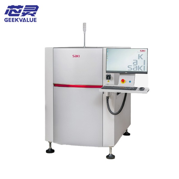
SAKI BF-10D is a high-precision 2D automatic optical inspection equipment (AOI) launched by SAKI of Japan, designed for ultra-precision PCB (such as IC substrate, FPC, high-density HDI board). Its core features are 10μm detection resolution and multi-spectral collaborative lighting system, which can cope with the complex defect detection needs of micro components (such as 01005, 008004) and highly reflective solder joints.
2. Working principle
2.1 Optical imaging system
Bright Field (bright field) multi-light source technology:
Adopt 8-directional programmable LED array (red/green/blue/white/infrared combination), through the reflection characteristics of different wavelengths of light sources, enhance the contrast between solder joints and substrates.
Coaxial optical path design: eliminate ambient light interference and ensure image stability.
High-resolution line scan camera:
Equipped with 10μm/pixel industrial-grade camera (optional 5μm/pixel), a single scan covers a larger field of view (FOV), taking into account both accuracy and efficiency.
2.2 Defect detection logic
Three-level detection algorithm:
Geometric matching: Compare the deviation of component position and contour with the standard template (such as offset and rotation).
Grayscale analysis: Identify cold solder joints, solder balls, bridges, etc. through the brightness distribution of solder joints.
AI classifier: Defect classification based on deep learning (such as the distinction between BGA solder ball collapse and normal depression).
3. Hardware design
3.1 Mechanical structure
Marble base + linear motor:
Zero thermal deformation base to ensure long-term stability (temperature drift <±2μm/℃).
Linear motor drive, scanning speed can reach 500mm/s, and repeated positioning accuracy is ±3μm.
Modular light source assembly:
Supports fast replacement of LED modules to adapt to different solders (such as lead-free SAC305 requires infrared auxiliary detection).
3.2 Core components
Components Specifications Function
Main camera 10μm/pixel CMOS linear array (12k pixels) High-precision image acquisition
Auxiliary camera 20μm/pixel global shutter array Quickly locate the mark point
Light source controller 16-channel independent PWM adjustment Dynamic control of lighting intensity/angle
4. Software functions
4.1 Detection function
Solder point detection:
SMT solder point: Identify BGA voids (detection rate>99%), QFN side solder point with less tin.
Through-hole solder point: Tin penetration rate analysis (support X-ray data fusion option).
Component detection:
01005 component tombstone, side flip, reverse polarity.
Connector pin coplanarity (simulate height through 2D image).
4.2 Intelligent assistance
SPI linkage: Automatically match solder paste printing data and predict potential defects (such as insufficient solder paste leading to cold soldering).
NG classification library: custom defect levels (Critical/Major/Minor), adapted to different customer standards.
5. Performance parameters
Category Parameters
PCB size Minimum 50mm×50mm, maximum 600mm×500mm (expandable)
Detection speed 0.15~0.3 seconds/detection point (depending on complexity)
Minimum component 008004 (0.25mm×0.125mm)
Communication protocol SECS/GEM, OPC UA, Modbus TCP
Power requirement AC 200V±10%, 50/60Hz, power consumption ≤2kW
6. Industry application
6.1 Typical scenario
IC substrate: Detection of copper foil residual glue and poor development of micro-pitch pads (≤50μm).
Flexible circuit (FPC): Solder cracking in the bending area (captured by multi-angle light source).
Automotive electronics: Reliability testing that meets AEC-Q100 standards (such as high-temperature solder cracks).
6.2 Customer Cases
A major semiconductor manufacturer: used for defect detection of 2.5D packaging interposer, with a false alarm rate of <0.05%.
Leading mobile phone manufacturers: Folding screen motherboard FPC detection, replacing the original 3D AOI solution to reduce costs by 30%.
7. Competitive advantages
Precision crushing the same level: 10μm resolution leads the market mainstream 20μm equipment (such as Omron VT-S730).
Light source flexibility: Multi-spectral combination solves the compatibility problem of high reflective/matte solder joints.
Open API: Support customer secondary development and customized detection logic.
8. Comparison of the upgrade points of BF-TristarⅡ
Features BF-10D BF-TristarⅡ
Resolution 10μm (optional 5μm) 10μm
Minimum component 008004 01005
Light source channel 16 channels programmable 8 channels fixed
Data interface OPC UA (Industry 4.0 compatible) SECS/GEM
9. Summary
SAKI BF-10D has become a benchmark 2D AOI equipment in the field of high-end PCB and semiconductor packaging with its "ultra-precision optics + multi-spectral collaboration + AI closed loop" technology combination, especially suitable for advanced manufacturing scenarios that pursue zero defects ppm.