 EN
EN id
id sk
sk sr
sr sv
sv it
it pt
pt bn
bn ms
ms be
be nl
nl fr
fr th
th vi
vi ru
ru ja
ja ko
ko de
de hy
hy az
az bs
bs bg
bg my
my cs
cs da
da dv
dv el
el et
et fil
fil fi
fi ga
ga gl
gl gn
gn he
he hi
hi km
km hr
hr hu
hu is
is kn
kn rw
rw lo
lo lv
lv lt
lt lb
lb lg
lg mi
mi mt
mt ne
ne no
no ny
ny or
or om
om per
per pl
pl ro
ro sa
sa so
so es
es sw
sw ta
ta tr
tr uk
uk ur
ur cy
cy xh
xh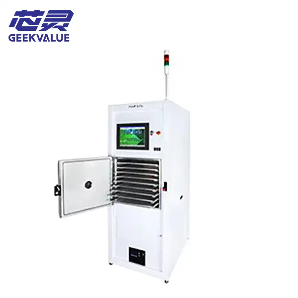
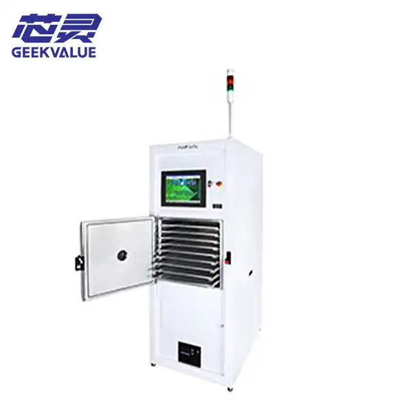 The IoN 200, introduced by PVA TePla, is an RF (Radio Frequency) plasma system specifically designed for surface modification, cleaning, and ashing applications. Its core strength lies in its exceptional flexibility: it not only meets the demands of R&D laboratories for precise process exploration but also integrates seamlessly into mass production environments, enabling the processing of large-format substrates and supporting high-volume manufacturing.
**Operating Principle**
The IoN 200 utilizes RF plasma technology to excite gases within a vacuum environment, thereby generating plasma. High-energy plasma radicals initiate both physical bombardment and chemical reactions on the material surface, thereby accomplishing process tasks such as cleaning, activation, or etching. Furthermore, PVA TePla offers an optional microwave plasma technology module; this technology harnesses electromagnetic wave energy to excite gases and generate reactive radicals. This ensures a cleaning process that is highly efficient, uniform, and isotropic, while effectively preventing ion-induced damage and electrostatic charge accumulation.
**Core Capabilities**
The IoN 200 possesses comprehensive process capabilities:
**Surface Cleaning:** Removal of non-volatile residues, such as organic contaminants and oxides.
**Surface Activation:** Introduction of polar functional groups to enhance surface wettability and adhesion, thereby preparing the surface for subsequent processes such as dispensing and bonding.
**Ashing / Descum:** In wafer manufacturing and packaging processes, this involves the precise removal of photoresist—or the clearing of residues remaining after pattern etching (i.e., descum)—through a highly efficient photoresist ashing process; this ensures damage-free, precision processing.
**Advantages and Features**
The table below highlights the outstanding technical advantages and design features of the IoN 200 across various dimensions:
**Dimension** | **Detailed Description**
**Exceptional Flexibility** | Capable of processing wafers up to 200 mm in diameter, as well as various types of large-format substrates. The system offers a variety of RF power supply options and supports the configuration of chambers and electrodes in various sizes to precisely match specific process requirements and production throughputs; notably, the largest chamber option boasts a capacity of up to 1,200 liters, providing ample room for future system expansion and upgrades.
**Robust Process Performance** | Utilizing RF plasma technology—and offering an optional microwave plasma module—the system demonstrates broad process adaptability. Its core objective is to ensure stable and consistent process results on substrates measuring up to 200 mm. For instance, during photoresist removal, the system achieves exceptional removal rates and uniformity.
**High Cleanliness & Environmental Friendliness:** The system employs a "dry" cleaning process—a stark contrast to traditional wet chemical cleaning methods—thereby eliminating the need to handle hazardous liquid waste and establishing itself as an environmentally friendly "green" technology.
**Leading Technology & Reliable Quality:** Drawing upon over 25 years of deep expertise in the field of plasma processing, PVA TePla is renowned within the industry for equipment lifetimes exceeding 20 years—a testament to its exceptional quality and reliability. Its unique microwave plasma technology enables comprehensive and damage-free cleaning of samples.
**User-Friendly Operation & Data Traceability:** The system’s design places a strong emphasis on versatile program control, fail-safe alarm systems, and data acquisition software. This not only provides users with an advanced and intuitive operational experience but also ensures process traceability, thereby meeting the industry's stringent requirements for quality control. **Technical Specifications**
While specific hardware specifications may vary depending on the actual configuration, the following core features of the IoN 200 are listed based on publicly available information:
**Parameter** | **Details**
**Device Type** | RF (Radio Frequency) Plasma Processing System (Optional Microwave Plasma System available)
**Wafer/Substrate Size** | Supports up to 200 mm (8 inches)
**Processing Mode** | Supports both Batch processing and Single-wafer/substrate processing modes to meet diverse process requirements regarding uniformity and cost-efficiency
**Chamber Configuration** | Modular design, compatible with various types of electrodes and chamber structures
**Key Applications** | Photoresist removal (Ashing/Stripping), Organic/Inorganic contaminant removal, Surface activation
**Process Gases** | Oxygen (O₂), Argon (Ar), Fluorine-containing gases, etc.
**RF Power** | Offers various power and frequency configuration options to suit specific process requirements (e.g., 13.56 MHz or 2.45 GHz [Microwave])
**Application Areas**
Leveraging its exceptional performance and flexibility, the IoN 200 plays a pivotal role across various high-end manufacturing sectors.
**Semiconductor Manufacturing (Front-end):** Used during the wafer fabrication process for photoresist ashing/stripping; for removing photoresist following processes such as ion implantation; and for eliminating organic and inorganic contaminants from wafer surfaces.
**Advanced Packaging (Back-end):** Employed to activate and clean substrate and chip surfaces prior to wire bonding, die attach, and underfilling, thereby ensuring optimal adhesion and filling results.
**MEMS and Optoelectronic Devices:** Utilized in the manufacturing of MEMS and optoelectronic components to remove sacrificial layers or photoresist residues—for instance, the removal of SU-8 photoresist.
**Other Industries:** Its underlying technological principles are also applicable to fields such as life sciences, medical technology, automotive electronics, and aerospace, where it serves to enhance product reliability and performance.
**Summary**
In summary, the PVA TePla IoN 200 is a powerful plasma processing system offering exceptional process flexibility. It delivers outstanding performance in high-quality cleaning, photoresist removal, and surface activation, making it particularly well-suited for laboratory R&D and medium-scale production environments involving substrates of 200mm or smaller. Its flexible modular design and robust performance establish it as a trusted solution within the semiconductor, microelectronics, and advanced packaging sectors.