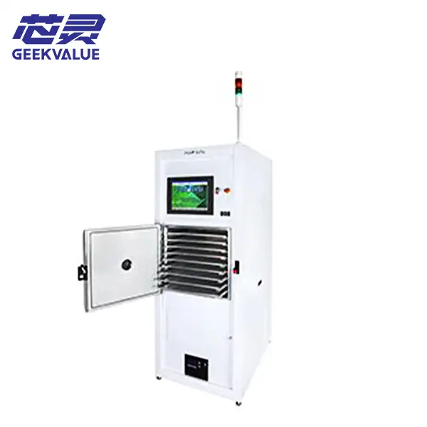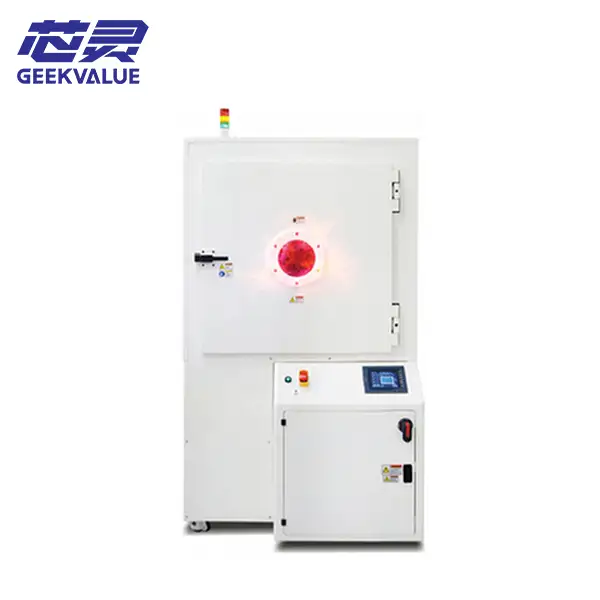
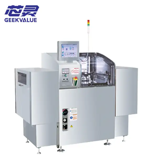
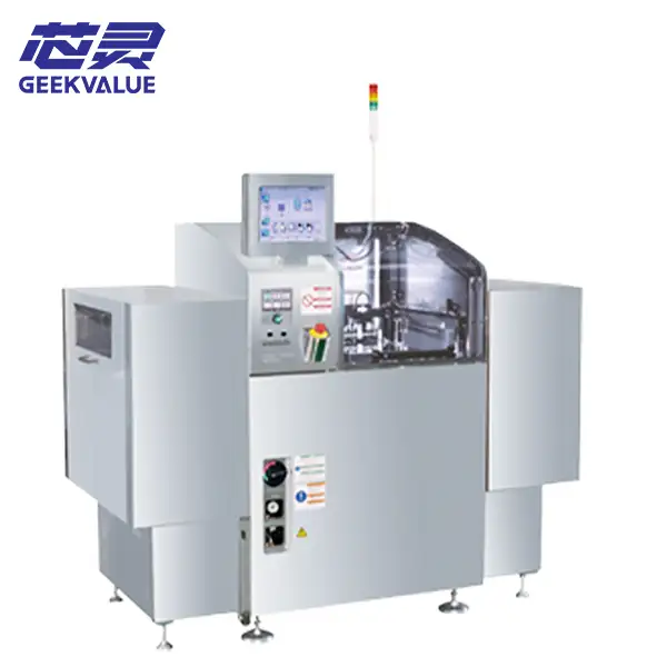
 The Panasonic PSX307 is an automated inline plasma cleaning system designed for substrates and wafers, specifically engineered to meet the high-throughput demands of modern semiconductor manufacturing. Leveraging cutting-edge parallel-plate electrode technology, this system boosts production efficiency by 1.5 times while simultaneously ensuring process quality; it delivers a high-performance solution designed to address the increasingly complex surface treatment challenges encountered in the field of advanced packaging.
**Operating Principle**
The PSX307 utilizes a 13.56 MHz Radio Frequency (RF) power source to generate a uniform plasma field via a parallel-plate electrode configuration. When process gases—such as argon—are ionized, the resulting high-energy particles achieve nanoscale cleaning and surface activation through the synergistic interplay of physical bombardment and chemical reactions. In terms of both efficiency and uniformity, this design offers fundamental advantages over traditional batch-type plasma systems. **Key Models and Product Positioning**
The PSX307 series comprises a range of models, designed to meet the diverse requirements of various production lines. A comparison of the core features for each model is provided below:
**Feature** | **S-Type** | **M-Type** | **PSX307A**
**Equipment Positioning** | Suitable for small to medium-sized substrates | Suitable for medium to large-sized substrates | Suitable for Wafer-Level Packaging (WLP)
**Processing Target** | Substrates (e.g., PCBs) | Substrates (e.g., PCBs) | Wafers up to 300 mm (with or without frames)
**Substrate Size Range** | L 50 x W 20 to L 250 x W 75 mm | L 50 x W 20 to L 330 x W 120 mm | Capable of simultaneously processing four substrates with a width of 77.5 mm
**External Dimensions (incl. Conveyor)** | W 2113 × D 1100 × H 1450 mm | W 2266 × D 1100 × H 1450 mm | Please refer to the technical specifications sheet for details
**Equipment Weight** | Approx. 850 kg | Approx. 725 kg | -
**Substrate Thickness** | 0.5 mm to 2.0 mm (for reference only) | 0.5 mm to 2.0 mm | -
**Detailed Specifications (PSX307 Base Model)**
**Parameter Category** | **Detailed Specifications**
**Equipment Model** | NM-EFP1A
**Cleaning Method** | Parallel-plate RF Back-sputtering
**Discharge Gas** | Argon (Ar) [Oxygen (O₂) optional]
**External Dimensions (Main Unit)** | W 930 × D 1100 × H 1450 mm
**Equipment Weight (Main Unit)** | Approx. 555 kg
**Power Supply Specifications** | Single-phase AC 200 V, 2.00 kVA (Peak 5.00 kVA)
**Gas Supply Requirements** | 0.49 MPa ...or higher; 6.5 L/min (A.N.R.)
**Core Functions and Technical Features**
Characterized by a high degree of automation and intelligence, the PSX307 demonstrates its technical superiority primarily through the following aspects:
**Chamber Design Balancing Uniformity and Etch Rate:** Ensures that every processing batch yields highly consistent etching results—a critical factor for process stability and yield.
**Panasonic’s Proprietary Plasma Monitoring Function:** Real-time monitoring and suppression of plasma discharge anomalies to prevent Electrostatic Discharge (ESD) damage, thereby ensuring "damage-free processing" of products.
**Traceability Function:** Provides comprehensive data tracking capabilities for the production process, meeting the stringent quality control requirements of the semiconductor manufacturing sector.
**In-line and Automated Transport:** Supports loader/unloader configurations and in-line specifications, allowing for direct integration into automated production lines without the need for manual intervention.
**Core Advantages and Application Fields**
Leveraging the aforementioned core technologies, the PSX307 demonstrates significant advantages in enhancing production quality and reducing costs, specifically in the following areas:
**Breakthrough Cost-Effectiveness:** By utilizing Argon (Ar) plasma processing technology to remove surface nickel compounds, it enables the adoption of the low-cost "Flash Gold" plating process. Concurrently, it effectively mitigates issues such as delamination, voids, and cracks that may arise during the packaging process. **Significant Efficiency Improvement:** Thanks to its in-line design combined with an automated transport system, the equipment achieves a processing speed of up to 360 substrates/strips per hour—representing a 50% increase in efficiency compared to conventional equipment.
Surface Modification to Meet Diverse Process Requirements:
**Improved Metal Bondability:** Prior to wire bonding or flip-chip assembly, the removal of organic contaminants significantly enhances shear strength and bonding reliability.
**Enhanced Resin Adhesion:** Surface modification utilizing oxygen plasma (O₂) doubles the adhesion strength of epoxy molding compounds and underfill materials, effectively preventing delamination.
**Optimized Underfill Processes:** Improves capillary flow characteristics, reducing underfill time by over 40%—a benefit particularly valuable for large-format chips and those with high I/O densities.
**Key Application Areas**
Thanks to its high-performance capabilities, the PSX307 is widely utilized in high-end semiconductor manufacturing processes:
**Wafer-Level Packaging:** Wafer surface modification prior to die bonding; cleaning of solder bumps before flip-chip bonding; and residue removal (desmearing) within TSV (Through-Silicon Via) structures.
**Advanced Packaging:** Cleaning and surface activation of PCB substrates prior to wire bonding, underfilling, and molding processes.
**Specific Processes & Materials:** Removal of resin residues from wafer solder bumps; improvement of the solderability of low-cost gold plating layers; and similar applications.
**Complementary Equipment**
As an integral part of Panasonic's semiconductor solutions portfolio, the PSX307 typically operates in tandem with Panasonic's high-precision MD-P series flip-chip bonders. This synergy ensures a seamless transition from cleaning to placement, resulting in a substantial improvement in overall product reliability.
**Summary**
In conclusion, the Panasonic PSX307 is a technologically advanced plasma cleaning system specifically engineered for mass production environments. Through the integration of innovative parallel-plate technology and a proprietary monitoring system, it achieves significant gains in production efficiency and effective reductions in manufacturing costs, all while ensuring a non-destructive process with exceptional uniformity. For applications involving large-format substrates or 300mm wafers—and where critical processes such as wire bonding and underfilling demand the highest levels of reliability—the PSX307 stands out as a solution well worth serious consideration.