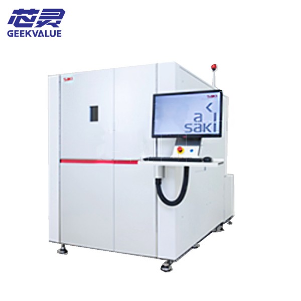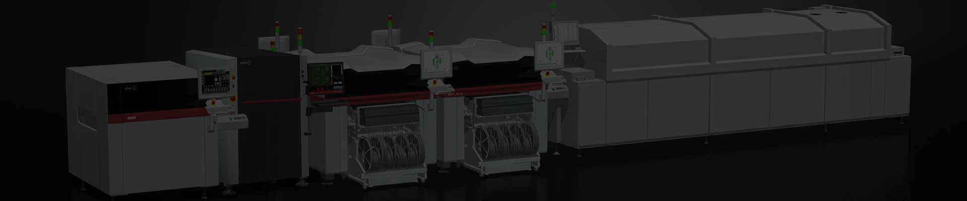
SAKI 3Si-MS2 is a high-precision 3D solder paste inspection system designed for modern SMT production lines. It uses multi-spectral 3D imaging technology to automatically detect the volume, height, and shape of solder paste after printing and before SMT, effectively preventing soldering defects and improving the pass yield (FPY). It is mainly used for process quality control of high-end PCBs such as mobile phone motherboards, automotive electronics, and servers.
2. Core technology principle
📌 3D imaging technology
Using laser triangulation + structured light projection dual mode:
Laser scanning (Laser Triangulation)
High-precision laser line scans the solder paste surface, captures reflected light through CCD camera, and calculates Z-axis height data
Accuracy of ±1.5μm (Z axis), suitable for ultra-fine pitch components (01005)
Structured light projection (Structured Light)
Multi-angle stripe light projection, enhances the 3D contour restoration ability of complex pads (such as BGA, QFN)
Solve the "shadow effect" problem of laser scanning on steep edges
📌 Intelligent detection process
PCB positioning → multi-spectral scanning → 3D modeling → AI defect analysis → SPC data feedback
3. Core functional features
🔹 1. Full parameter solder paste detection
Detection items Measurement accuracy Process significance
Volume (Volume) ±3% Ensure sufficient tin to avoid cold soldering or insufficient tin
Height (Height) ±1.5μm Control solder paste collapse and prevent bridging
Area: ±5μm Identify printing offset or stencil blockage
Shape: 3D contour comparison Detect molding defects such as pull tip and depression
🔹 2. Advanced defect detection capabilities
Typical defect coverage:
✅ Insufficient Paste
✅ Bridging
✅ Misalignment
✅ Peaking/Dimming
✅ Stencil Contamination
Special scene detection:
✔ Thickness difference compensation for step stencil
✔ Solder paste pull tip identification for fine pitch QFN
🔹 3. Intelligent data analysis
Real-time SPC control: Automatically generate CPK/PPK reports to monitor printing process stability
Closed-loop feedback: Automatically adjust printer parameters (such as scraper pressure and speed)
4. Hardware specifications and configurations
📌 Optical system
Components Parameters
Laser source 650nm red laser, scanning frequency 20kHz
Structured light projection Blue LED stripe light, resolution 5μm
Camera 5 million pixel high-speed CMOS, frame rate 120fps
Light source system Ring LED + coaxial light combination, 8 adjustable lighting modes
📌 Mechanical performance
Project Specifications
Detection speed Maximum 45cm²/s (high-speed mode)
PCB size range 50mm×50mm ~ 510mm×460mm
Minimum detection element 01005 (0.4mm×0.2mm)
Repeat accuracy X/Y: ±3μm, Z: ±1.5μm
Motion system High rigidity linear motor, acceleration 1.5G
📌 Software platform
SAKI VisionPro operating system
Graphical programming interface, support offline simulation (OLP)
AI self-learning function: automatic optimization of detection threshold
Report output format: PDF/Excel, support for custom templates
5. Product core advantages
✅ Balance of precision and speed
Z-axis precision ±1.5μm, while maintaining a detection speed of 45cm²/s, 20% faster than similar equipment
Automatic switching of dual scanning modes (laser + structured light), taking into account both efficiency and accuracy
✅ High degree of intelligence
Deep learning algorithm: automatic classification of defect types, false alarm rate <2%
Adaptive lighting: eliminate PCB color/reflective interference
6. Typical application cases
📱 Consumer electronics
Mobile phone motherboard: detection of solder paste printing of 0.3mm pitch CSP devices
TWS earphone charging box: volume control of tiny pads (0.2mm diameter)
🚗 Automotive electronics
ADAS module: ensure BGA solder paste filling rate >90% (compliant with IPC Class 3)
In-vehicle display: FPC flexible board printing quality monitoring
🖥️ Industrial equipment
Server CPU socket: coplanarity detection of large-size pads
5G base station PA module: solder paste molding control of high-frequency materials
7. Advantages compared with competing products
Dimension SAKI 3Si-MS2 Conventional 3D SPI 2D SPI
Detection technology Laser + structured light dual mode Single laser scanning Planar imaging only
Z-axis accuracy ±1.5μm ±3~5μm Unable to measure
Speed 45cm²/s Usually 30~35cm²/s Faster but limited in function
Defect recognition AI classification of 20+ defects Basic algorithm (5-10 types) Only contour analysis
8. Summary
SAKI 3Si-MS2 provides high-density SMT production with multi-spectral 3D imaging + AI intelligent analysis:
Process prevention: intercept more than 95% of solder paste defects before patching
Data empowerment: real-time SPC drives printing process optimization
Flexible adaptation: full coverage detection from 01005 to large BGA
")