Tray to Tray
Singulated packaged devices or delicate components loaded in JEDEC or custom trays.
Tray geometry, pocket depth, pickup surface and device orientation determine whether the existing loader, nest and vision setup can be reused.
ave up to 70% on SMT Parts – In Stock & Ready to Ship
Get Quote →A semiconductor chip handler moves devices from their incoming media to inspection, electrical test or finishing stations, keeps each chip correctly oriented and traceable, then places it into the required output bin, tray, tube or tape. The right machine depends on where the device starts, how fragile it is, what operations must happen in the middle and how the accepted and rejected chips should leave the system.
Two machines may both be called semiconductor chip handlers while using completely different loading, motion and output systems. Begin with the device media and destination before comparing speed or brand.
Singulated packaged devices or delicate components loaded in JEDEC or custom trays.
Tray geometry, pocket depth, pickup surface and device orientation determine whether the existing loader, nest and vision setup can be reused.
Devices supplied in tubes, feeders or bulk-oriented input for high-speed finishing.
The route must keep devices oriented from bulk or tube input through indexing, inspection or test, then place each result into the correct tape pocket or reject output.
Diced devices remain on film frame after singulation and must be picked without damaging the die or package.
Wafer-map data, ejector support, pickup force and die orientation must remain linked when devices move from film frame to tray, tape or reconstructed-wafer output.
Devices are tested or inspected before complete singulation or while mounted on a carrier.
Strip size, carrier support, contact layout and post-test separation determine whether the platform can process the product before or after singulation.
Individual devices rotate through multiple stations for test, inspection, marking and sorting.
The useful configuration depends on station order, pickup method, inspection and tester connections, marking requirements and the final bin, tray or tape route.
Browse the current collection, then confirm the input media, device size, required stations, output format and installed conversion hardware for the actual machine.
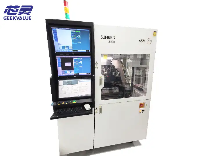
SUNBIRD provides an efficient, reliable and flexible wafer testing solution for the semiconductor industry through innov...
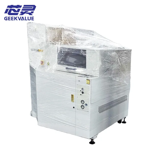
As an upgraded version of the MS100, the ASM MS100 Plus is also a device for chip sorting and arrangement based on wafer...
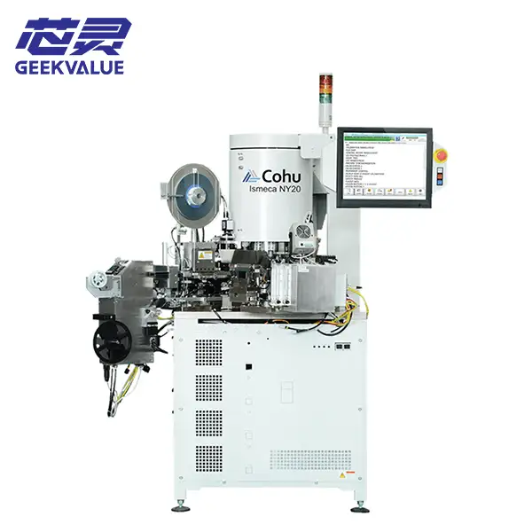
The ISMECA NY20 (now owned by Cohu) is a 20-station rotary ultra-high-speed semiconductor testing and sorting machine
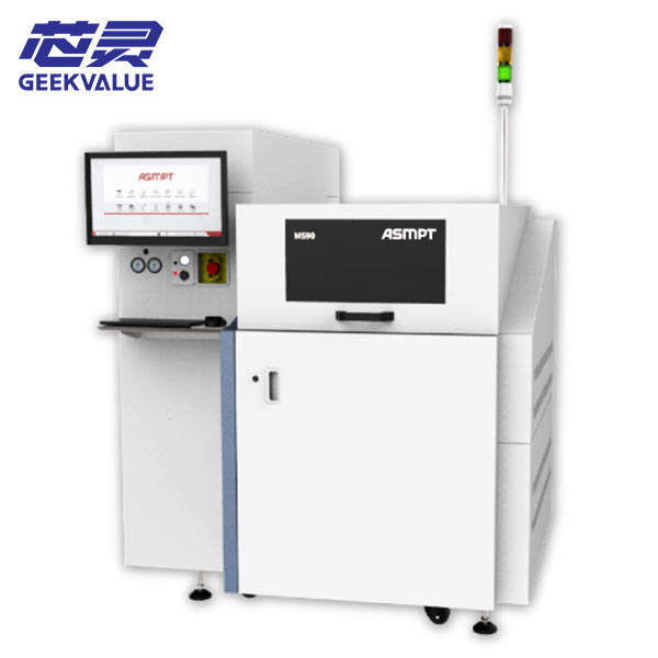
ASM sorting machine MS90 is a device designed for lamp bead sorting, with efficient and accurate sorting functions. This...
High throughput is useful only when the handler protects the device, preserves lot identity and presents each chip correctly to the next operation. These risks often determine the real machine configuration.
Bare die, WLCSP, thin packages, MEMS, sensors and optoelectronic devices may require controlled vacuum, compliant contact, edge support or a dedicated pickup surface.
The system must recognize the device, verify orientation and place it consistently before inspection, electrical contact, marking or output packing.
Map position, barcode, OCR, recipe, bin result and output location may need to remain linked throughout the handling route.
Socket alignment, contact force, coplanarity and dwell time affect repeatability even when the electrical measurement is performed by separate ATE.
Accepted, rejected and graded devices may leave through different trays, tubes, bins, reels or reconstructed wafer positions.
VISIONTop, bottom, sidewall, bump, lead or code inspection may be added before or after testing.
TESTThe handler places the device at the contact interface while the ATE or dedicated tester performs the measurement.
THERMALTemperature capability must match the device power, test time, thermal soak method and required accuracy.
MARKSome finishing handlers integrate marking, code verification and reinspection before output.
PACKThe final pack format and grade logic should be defined before conversion kits and automation are selected.
The term chip handler can describe more than a simple transport machine. Depending on the platform, it may present devices to electrical test, rotate them through inspection stations, apply marking, classify results and prepare the final output media.
A semiconductor device handler is useful only when its installed tooling can carry your device from the actual incoming media through the required stations and into the correct output. Define that route before comparing model names or advertised speed.
Record package or die dimensions, thickness, weight, warpage, fragile surfaces and the face that may safely contact a nozzle, gripper, nest or ejector.
State whether devices arrive in trays, tubes, strips, bowls, carriers or film frames, including pocket geometry, orientation and unloading constraints.
Define polarity, rotation, wafer-map use, barcode or OCR requirements and the point at which the machine must confirm device identity.
List inspection, electrical test, thermal conditioning, marking, reinspection and grading in the order the device must visit them.
Explain how pass, fail, recheck, visual defect, electrical bin or customer grade should control the next destination.
Confirm tray, tube, reel, reconstructed wafer or bin output together with tester, MES, traceability and factory-utility connections.
These questions focus on device movement and output integrity rather than repeating the general Test Handler, machine-structure or IC-package pages.
The terms often overlap. A test handler is specifically used to automate device presentation, temperature control and sorting around electrical final test. The broader term semiconductor chip handler may also be used for platforms that combine transport with vision inspection, marking, packaging or other finishing operations. The actual station list must be checked for each machine.
Some platforms are designed for singulated packaged ICs, while others can pick diced die directly from film frame or handle delicate wafer-level packages. Suitability depends on the pickup method, device support, ejector, vision, handling force and output media.
Possible formats include trays, tubes, strips, carriers, film frames, bowls, tape and reel, reconstructed wafers and multiple sorting bins. No machine should be assumed to support all formats without confirming the installed modules and conversion kits.
Common causes include unsuitable pickup force, worn nozzles or nests, incorrect vacuum, device warpage, contaminated optics, unstable motion, poor lighting, wrong recipe data and mismatched conversion tooling.
Often it can, but the conversion may require new pick heads, nozzles, nests, feeders, trays, guides, contact hardware, cameras, software or output modules. The conversion cost should be reviewed before the machine is purchased.
Send the device drawing or package size, starting media, required operations, output media, tester or inspection requirement, temperature range, throughput target, preferred condition, quantity and destination.

Share the device, incoming media, required inspection or test stations, output format, throughput target and destination. We will review the available semiconductor chip handler equipment and the conversion work that may be required.
Why do so many people choose to work with GeekValue?
Our brand is spreading from city to city, and countless people have asked me, "What is GeekValue?" It stems from a simple vision: to empower Chinese innovation with cutting-edge technology. This is a brand spirit of continuous improvement, hidden in our relentless pursuit of detail and the delight of exceeding expectations with every delivery. This almost obsessive craftsmanship and dedication is not only the persistence of our founders, but also the essence and warmth of our brand. We hope you will start here and give us an opportunity to create perfection. Let us work together to create the next "zero defect" miracle.
DetailsContact a sales expert
Reach out to our sales team to explore customized solutions that perfectly meet your business needs and address any questions you may have.