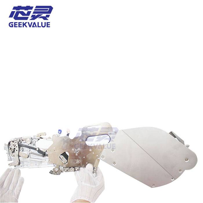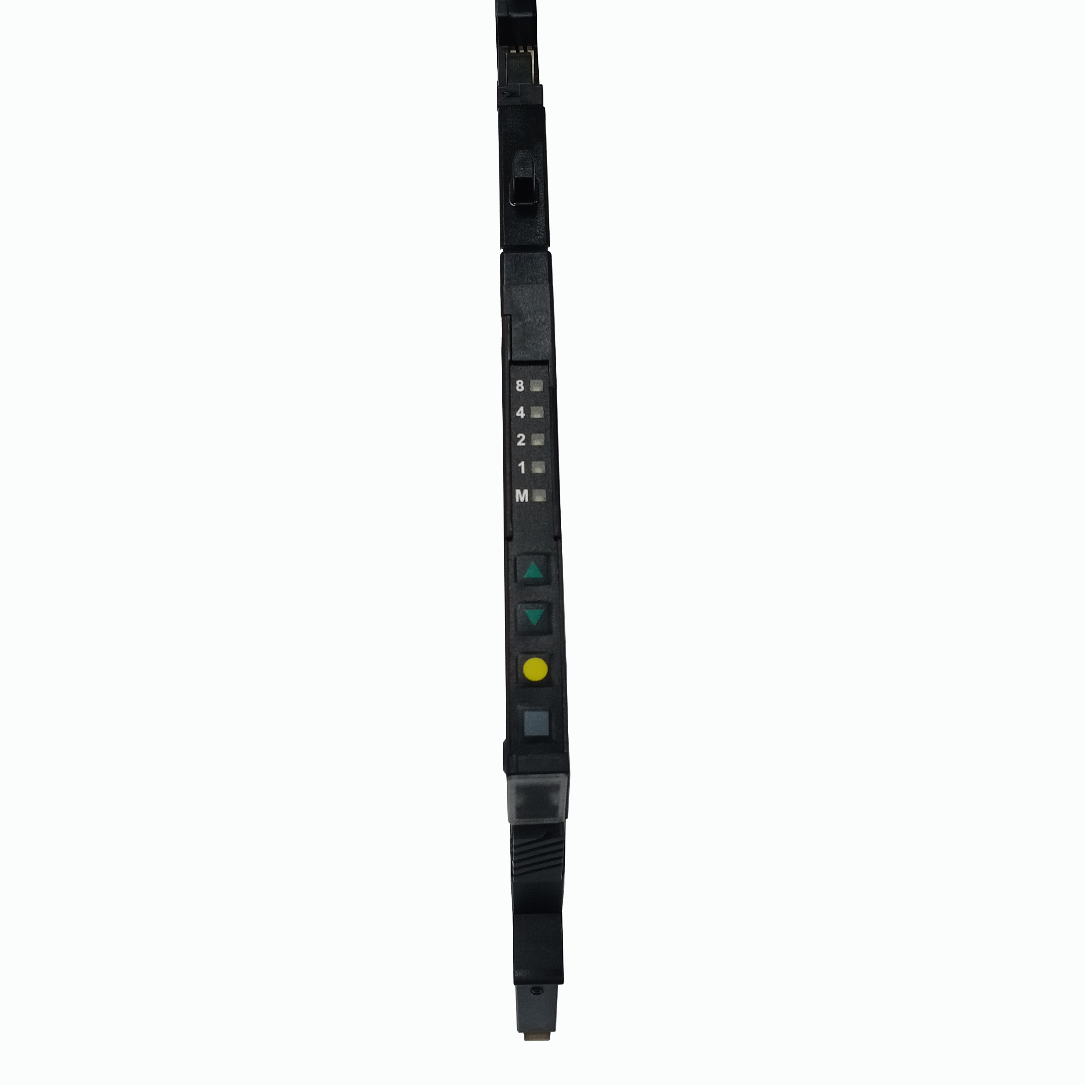
Modern System-in-Package and advanced packaging products often require several very different component types to be assembled on the same substrate. Passive components and packaged ICs may arrive in tape-and-reel feeders, while bare semiconductor dies must be picked directly from a sawn wafer, inspected, oriented and placed with much tighter process control.
The ASM SIPLACE CA2 was developed for this mixed production environment. Instead of separating standard SMT placement and direct-wafer die processing into completely independent equipment stages, the CA2 combines both material flows within one advanced placement platform. It can process feeder-supplied SMDs, perform die attach from wafer and handle flip-chip placement for compact, highly integrated electronic assemblies.
This makes the SIPLACE CA2 especially relevant for manufacturers evaluating semiconductor die bonder equipment for SiP modules, power electronics, embedded components, wafer-level packaging and other applications where conventional SMT capability alone is not sufficient.
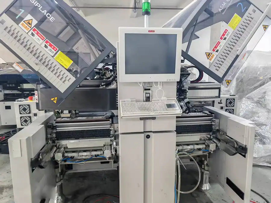
What Type of Machine Is the ASM SIPLACE CA2?
The SIPLACE CA2 is best described as a high-speed hybrid placement platform for semiconductor and SMT assembly. It is not limited to a single material source or one traditional packaging process.
Depending on the installed machine configuration, the CA2 can coordinate several production tasks:
Pick standard SMD components from tape-and-reel feeders.
Remove known-good dies directly from a sawn wafer.
Place bare dies in die-attach orientation.
Turn and place dies for flip-chip assembly.
Process components supplied through trays or specialized carriers.
Apply flux or other dipping media before placement.
Inspect dies and components during the placement process.
Record the relationship between the original wafer position and final substrate position.
The result is a production platform that can connect processes traditionally associated with an SMT placement machine and a semiconductor die bonder.
Why Advanced Packaging Lines Need a Hybrid Placement Platform
A conventional SMT line is highly efficient when most materials are supplied in standardized feeders. Advanced packaging introduces a different challenge because the final product may combine passives, packaged semiconductors, sensors, power dies and unpackaged ICs on one substrate.
When these materials are processed on separate equipment, production may require additional transfers, intermediate storage, separate programming environments and more complex traceability. Bare dies may also need to be converted into tape packaging before they can enter a conventional SMT placement process.
The SIPLACE CA2 addresses this production gap by bringing direct-wafer handling into an SMT-oriented platform. Dies can be taken from the wafer and introduced into the placement sequence together with feeder-supplied components, reducing the number of disconnected process stages.
CA2 Compared with a Conventional Split Production Route
| Production Requirement | Conventional Split Process | ASM SIPLACE CA2 Approach |
|---|---|---|
| Standard SMD placement | Processed on an SMT placement machine | Processed from compatible tape-and-reel feeders |
| Bare die handling | Normally transferred to a separate die bonder | Dies can be picked directly from the sawn wafer |
| Flip-chip placement | May require dedicated semiconductor assembly equipment | Supported within the configured CA2 process flow |
| Die material preparation | Dies may need to be repacked or transferred before placement | Direct wafer processing can reduce additional material conversion |
| Process data | Information may be distributed across separate equipment systems | Supports die-level tracking from wafer source to placement position |
| Line integration | SMT and semiconductor assembly areas may operate independently | Designed for integration into connected advanced packaging lines |
The most suitable production route still depends on product volume, die range, process chemistry, substrate design and existing factory infrastructure. The CA2 is particularly valuable when both SMT components and wafer-supplied dies must be processed repeatedly within the same product family.
ASM SIPLACE CA2 Main Specifications
| Specification | Published CA2 Capability |
|---|---|
| Machine category | Hybrid SMT placement, die-attach and flip-chip platform |
| Maximum SMT placement speed | Up to 76,000 components per hour |
| Maximum die-attach speed from wafer | Up to 54,000 dies per hour |
| Maximum flip-chip speed from wafer | Up to 51,000 dies per hour |
| Standard placement accuracy | 20 µm at 3 sigma |
| Additional accuracy classes | 15 µm and 10 µm at 3 sigma |
| Wafer capacity | Up to 50 different wafers with the applicable wafer exchange configuration |
| Wafer exchange time | Less than 13 seconds under the specified configuration |
| Maximum single-lane substrate format | Up to 620 × 700 mm, depending on selected accuracy and conveyor configuration |
| Dual-lane substrate formats | Configuration-dependent formats for standard PCBs and SiP substrates |
| Machine dimensions | Approximately 2.56 × 2.50 × 1.85 m |
| Factory communication | IPC-HERMES-9852, IPC-2591 CFX, IPC-SMEMA-9851 and SECS/GEM |
| Production environment | Cleanroom-compatible configuration and semiconductor production standards support |
Published maximum values describe the platform capability. Actual production output depends on the installed head, die dimensions, wafer condition, substrate design, process options, inspection requirements and component mix.
Direct Wafer Processing and Material Flow
One of the most important CA2 capabilities is its ability to process dies directly from a sawn wafer. In a traditional feeder-based workflow, bare dies may first need to be transferred into tape or another standardized carrier before placement.
Direct wafer processing can remove or reduce that intermediate conversion step. This may provide several operational benefits:
Fewer tape-related preparation and material-handling operations.
Reduced storage requirements for converted die materials.
Less tape and carrier waste associated with repackaging dies.
Fewer replenishment and splicing activities for die materials.
Better connection between wafer-map data and final placement records.
More flexible use of multiple dies within complex SiP products.
The CA2 uses wafer-handling and die-buffering functions to separate time-consuming die preparation from the placement sequence. This parallel process helps maintain production output while dies are being prepared for pickup and placement.
Die Attach and Flip-Chip Production
Die-Attach Placement
In a die-attach process, the semiconductor die is removed from the wafer and placed in the required orientation on the substrate. Depending on the product and machine options, the process may include material dipping, die inspection and controlled low-force placement.
Flip-Chip Placement
Flip-chip assembly requires the die to be correctly oriented so its active side and interconnection structure face the substrate. Placement accuracy, die condition, flux transfer and substrate mapping become especially important when bump dimensions and component spacing are small.
Mixed SMT and Die Placement
The CA2 can combine wafer-supplied dies with conventional components picked from compatible ASM SMT feeders. This allows one product to include resistors, capacitors, packaged ICs and several bare die types without treating every material group as a completely separate assembly project.
Placement Head and Accuracy Options
The machine can be equipped with a CP20 placement head for high-speed and high-accuracy component handling. The CP20 is intended for small and sensitive components and supports touchless pickup and zero-force placement functions.
Published CP20 capabilities include:
Component range beginning at 0201 metric.
Maximum component dimensions up to approximately 8.2 × 8.2 mm.
Component height up to approximately 4 mm.
Placement output up to 38,000 components per hour per applicable head configuration.
Accuracy capability down to ±10 µm at 3 sigma.
The required accuracy class should be selected according to die dimensions, interconnection pitch, ball or bump size, substrate tolerance and product yield requirements. A machine configured for standard 20 µm placement should not automatically be assumed to provide the optional 10 µm process class.
Wafer Exchange and Multi-Die Production
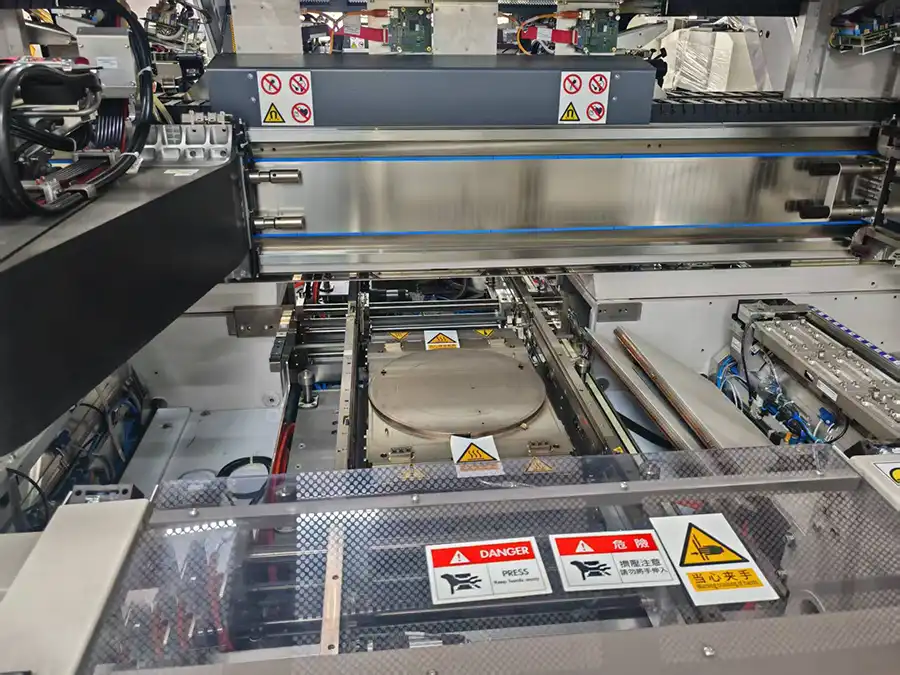
Complex SiP products may contain several different dies. Changing wafer materials manually for every die type would create a major production bottleneck. The CA2 wafer exchange system is designed to maintain multiple wafer types and present the required material to the placement process as the production program changes.
With the applicable configuration, the wafer system can hold up to 50 different wafers. This multi-die capability is particularly useful for products that combine processors, memory, sensors, communication dies and power components in one compact package.
When evaluating an available machine, confirm:
The installed wafer exchange system and number of supported wafer positions.
Supported wafer diameters and wafer-frame specifications.
Wafer ejector, die-flip and buffer-module configuration.
Compatibility with the required wafer-map format.
Maximum and minimum die dimensions.
Supported die thickness and die condition.
Available bad-die recognition and known-good-die data.
Substrate and Conveyor Configurations
The CA2 can be configured for different substrate flows rather than being restricted to one conventional PCB format.
Single-Lane Conveyor
A single-lane configuration can support large panels, embedded PCBs and specialized substrates. Published formats reach up to 620 × 700 mm for selected accuracy classes and machine arrangements.
Dual-Lane Conveyor
Dual-lane transport is suited to standard PCBs and SiP substrates where parallel board handling can improve line utilization. Supported dimensions vary with the selected conveyor mode and accuracy requirement.
Chip-on-Wafer and Specialized Carriers
Available options may also support chip-on-wafer processes, JEDEC trays, J-boats, thick boards and warped substrates. These functions must be checked against the actual installed machine configuration.
Inspection, Dipping and Process Control
High placement speed alone is not sufficient for advanced packaging. The process must also verify die condition, pickup quality, orientation and material application.
Depending on the selected options, the CA2 can support:
Component presence and pickup detection.
Die-crack and die-chipping inspection.
Flux or dipping-material detection.
Solder-paste inspection before or after placement.
Substrate mapping and placement-position correction.
Process data exchange with factory systems.
Closed-loop production functions when compatible inspection equipment is installed.
A Linear Dipping Unit may be used where dies require flux or another transfer medium before placement. The selected dipping plate, material properties, transfer height and inspection settings should be qualified for the actual die and substrate process.
Single-Die-Level Traceability
Semiconductor assembly often requires more detailed material records than conventional component-lot tracking. The CA2 supports tracking an individual die from its original position on the wafer to its final location on the assembled substrate.
This can help production teams connect:
Wafer identification and wafer-map information.
Original row and column position of the die.
Die pickup and inspection results.
Final board or substrate serial number.
Placement coordinates in the completed product.
Process and equipment data collected during assembly.
The final traceability scope depends on the installed software, factory interfaces, customer database and production-system integration.
Integration with an Advanced Packaging Line
The SIPLACE CA2 can be used as a central hybrid placement machine or combined with additional high-speed and high-accuracy equipment. ASMPT identifies the SIPLACE TX micron as a complementary platform for SiP production where both machines are arranged within the same line.
A line configuration may include:
Substrate loading and identification.
Solder paste, adhesive or flux application.
Inspection of the printed or dispensed material.
High-speed placement of conventional SMD components.
Direct-wafer die attach or flip-chip placement on the CA2.
Post-placement inspection.
Reflow, curing or subsequent packaging processes.
Final inspection, test and traceability recording.
The correct line design depends on process sequence, takt time, substrate handling, cleanroom requirements and whether the CA2 performs all placement steps or only the specialized die-processing operations.
Typical Products and Applications
System-in-Package modules: Assemblies combining several bare dies, packaged ICs and passive components.
Communication modules: Compact RF, 5G, network and wireless electronic packages.
Automotive electronics: Sensor, control and high-integration modules requiring detailed traceability.
Power semiconductor products: Power dies and supporting SMD components assembled on specialized substrates.
Wafer-level packaging: Processes involving placement on wafers or wafer-derived substrates.
Panel-level packaging: Advanced packaging on larger-format panels.
Embedded electronics: Components and dies placed into or onto embedded PCB constructions.
Sensor and medical modules: Compact assemblies containing sensitive bare dies and control electronics.
Computing and smart-device modules: High-density products requiring multiple component formats.
When Is the SIPLACE CA2 a Suitable Choice?
The CA2 should be considered when the production requirement includes several of the following conditions:
The product combines feeder-supplied SMDs and bare dies.
Dies must be picked directly from one or more wafers.
Die attach and flip-chip processes are required in the same product family.
Production requires multiple die types with frequent material changes.
Placement accuracy must reach 20 µm, 15 µm or 10 µm process classes.
Single-die traceability is required.
The manufacturer wants to reduce die taping and intermediate material handling.
The equipment must communicate with both SMT and semiconductor factory systems.
Large panels, SiP substrates or specialized carriers must be processed.
A dedicated die bonder may still be more appropriate when the application requires specialized bonding force, heating, curing, dispensing or die sizes outside the available CA2 configuration. A process review should therefore be completed before selecting the machine.
Available ASM SIPLACE CA2 Equipment
Used or pre-owned SIPLACE CA2 machines may differ significantly even when the exterior model designation is the same. The installed wafer system, placement head, conveyor, accuracy class, inspection options and software determine what the individual unit can process.
Before quotation, the following equipment information should be confirmed:
| Inspection Item | Information to Verify |
|---|---|
| Machine identity | Full model, serial number, manufacturing year and nameplate photographs |
| Placement system | Installed CP20 heads, head labels, operating hours and available calibration information |
| Accuracy configuration | 20 µm, 15 µm or 10 µm machine class and supported substrate area |
| Wafer handling | Wafer exchange unit, buffer, ejector, flip unit and supported wafer formats |
| Conveyor | Single-lane, dual-lane or specialized substrate transport |
| Process modules | Dipping, inspection, traceability and chip-on-wafer options |
| Software | Installed software version, licenses, communication interfaces and program availability |
| Supply scope | Feeders, nozzles, wafer accessories, documentation, spare parts and export packing |
| Machine condition | Used, tested, serviced or refurbished condition and available running information |
Machine, Feeder and Spare-Parts Support
Equipment supply can be matched to the required substrate size, wafer format, component range, accuracy level and process application. Depending on availability, support may include:
Complete ASM SIPLACE CA2 machines.
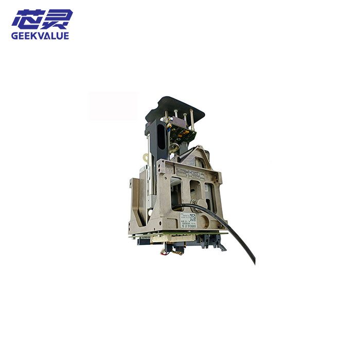
Compatible placement heads and head components.
Wafer exchange and wafer-handling parts.
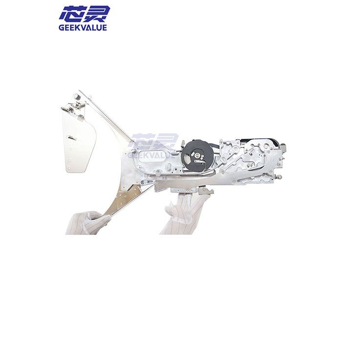
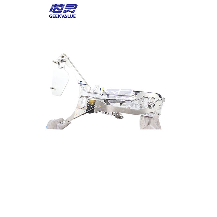
ASM SIPLACE feeders and feeder spare parts.
Standard and application-specific nozzles.
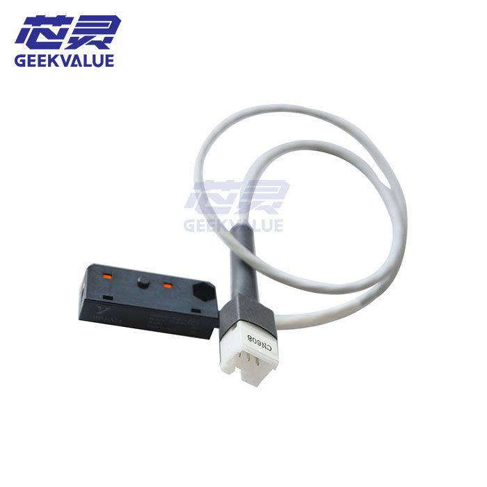
Cameras, sensors and inspection components.
Motors, drives, control boards and cables.
Conveyor and substrate-handling components.
Installation, packing and international shipment support.
Information Required for Equipment Matching
For a more accurate machine recommendation, provide:
Product and process description.
Required die-attach, flip-chip or mixed placement process.
Die dimensions, thickness and wafer diameter.
Number of different die types per product.
Smallest and largest SMD package.
Substrate dimensions, thickness and material.
Required placement accuracy.
Expected hourly or annual production volume.
Required feeder, tray and wafer capacity.
Factory interface and traceability requirements.
Preferred equipment condition and destination country.
Frequently Asked Questions About the ASM SIPLACE CA2
What production problem does the SIPLACE CA2 solve?
It addresses products that require both conventional SMT components and bare semiconductor dies. The CA2 brings feeder-based component placement and direct-wafer die processing into a coordinated machine platform.
Can the CA2 replace every conventional die bonder?
No single machine is suitable for every semiconductor process. The CA2 is optimized for high-speed hybrid placement, die attach and flip-chip applications. Processes requiring specialized heating, bonding force, curing or unusual die formats must be evaluated separately.
Does the machine require dies to be supplied in tape?
No. One of its main capabilities is picking dies directly from a sawn wafer. It can also process standard SMD components supplied through compatible tape-and-reel feeders.
Can several different wafers be used in one production setup?
Yes. With the applicable wafer exchange system, the machine can accommodate up to 50 different wafers, making it suitable for multi-die products.
What is the difference between die attach and flip-chip placement on the CA2?
Die attach places the die in the required face-up orientation, while flip-chip processing turns and places the die with its interconnection side facing the substrate. The exact sequence depends on the installed modules and product process.
Can the CA2 work in the same line as a SIPLACE TX micron?
Yes. The two platforms can complement each other in advanced packaging and SiP lines, with the TX micron supporting high-speed, high-accuracy placement and the CA2 handling direct-wafer and hybrid placement processes.
Does the CA2 support cleanroom production?
The platform is available with cleanroom-compatible and semiconductor-standard configurations. The certification and condition of an individual used machine should be confirmed before purchase.
How should a used SIPLACE CA2 be evaluated?
Review the machine identification, placement heads, accuracy class, wafer modules, conveyor, software, inspection functions, operating condition and included accessories. The model name alone does not define the complete process capability.
Are feeders and wafer accessories included?
The supply scope varies by machine and quotation. Feeders, nozzles, wafer frames, handling accessories and spare parts should be listed individually in the final equipment offer.
What information should be sent with an inquiry?
Provide the die and wafer specifications, component range, substrate dimensions, required process, accuracy target, production output, preferred machine condition and delivery destination.
Contact us with your wafer format, die range, substrate size and required assembly process to check available ASM SIPLACE CA2 configurations and supply options.