Turret Test and Vision Handler
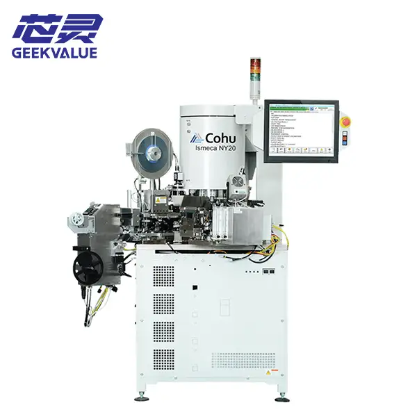
ISMECA test handler NY20
The ISMECA NY20 (now owned by Cohu) is a 20-station rotary ultra-high-speed semiconductor testing and sorting machine
ave up to 70% on SMT Parts – In Stock & Ready to Ship
Get Quote →A turret test and vision handler combines semiconductor electrical test, optical inspection, defect classification and production sorting on one configurable platform. The correct system depends on the package surfaces that must be inspected, the electrical test requirement, the input and output media and the camera, lighting, software and test stations installed on the machine.
Vision capability should be selected from the package, defect type and quality gate, not from the number of cameras alone. Leaded devices, WLCSP, sensors and power packages may require different optics, lighting, image angles and measurement algorithms.
Confirm OCR or code reading, contrast, missing marks, position and verification after laser marking.
Evaluate scratches, contamination, flash, chipping, cosmetic limits and visible evidence of molding defects.
Inspect lead damage, pad contamination, bent terminals, pitch, coplanarity and dimensional tolerance.
Some applications require infrared or other specialized methods rather than standard visible-light imaging.
Inspection scope is not a fixed machine sequence. Select the required surfaces, measurements and packing checks first, then verify that the supplied handler includes the necessary camera positions, optics, lighting and software licenses.
Browse the current equipment collection. Machines from the same platform may include different test stations, cameras, optics, lighting modules, inspection licenses and conversion tooling. Confirm the configuration of the individual machine before arranging an inspection trial.
The ISMECA NY20 (now owned by Cohu) is a 20-station rotary ultra-high-speed semiconductor testing and sorting machine
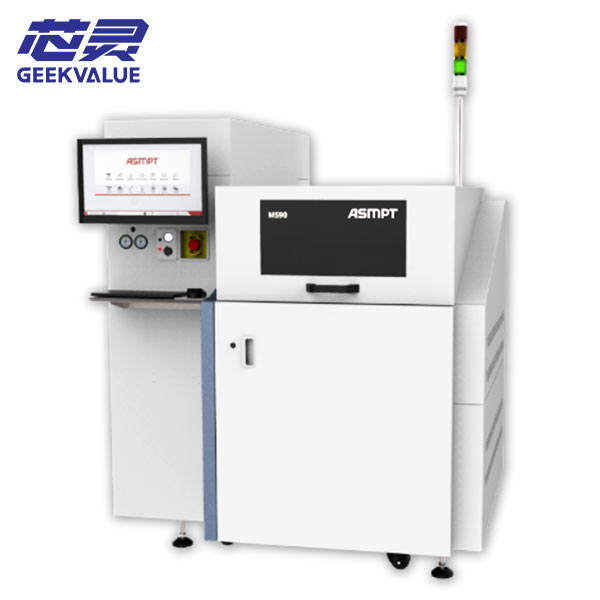
ASM sorting machine MS90 is a device designed for lamp bead sorting, with efficient and accurate sorting functions. This...
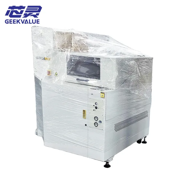
As an upgraded version of the MS100, the ASM MS100 Plus is also a device for chip sorting and arrangement based on wafer...
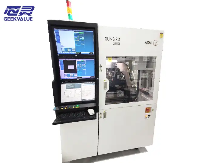
SUNBIRD provides an efficient, reliable and flexible wafer testing solution for the semiconductor industry through innov...
A passing electrical test does not prove that the package surface, leads, marks or packing condition meet the outgoing quality requirement. The handler must coordinate both result streams without mixing their responsibilities.
The answer depends on the tester, interface, contactor, test program, stable contact and the actual test stations installed on the handler.
The answer depends on camera position, lens, lighting, resolution, calibration, image algorithm and inspection recipe.
Sorting rules may separate electrical failure, visual failure, recheck, grade and accepted output into different bins or packaging routes.
Vision inspection can mean a basic top-camera check or a multi-station system that measures several package surfaces and dimensions. Select the required inspection stack before comparing handler throughput.
Useful for orientation, printed codes, visible damage, contamination and basic dimensional checks.
Used when package geometry, bump or lead height and dimensional variation influence acceptance.
Supports broader defect screening for leaded, leadless, WLCSP, discrete and sensor packages.
May be required for microcracks, hidden features, material contrast or package-specific inspection tasks.
Strong inspection performance is not only a question of finding defects. It also requires stable presentation, repeatable lighting, correct calibration and a recipe that separates true failures from harmless variation.
Orientation, pocket position, suction stability and motion repeatability affect image consistency.
Lens, angle, intensity and wavelength must match the surface finish and defect type.
Thresholds, measurement windows and classification rules should reflect the actual package standard.
Record recipe versions, calibration status and approved parameter changes so results remain comparable after maintenance or product conversion.
Camera count and nominal resolution do not prove inspection capability. Before accepting a machine, run representative good devices, known defect samples and boundary-condition parts through the actual optics, lighting and inspection recipe.
Include normal good devices, confirmed defects, boundary-condition parts and expected variation from different lots. Cover every surface, orientation and defect family included in the acceptance standard.
Run the same samples through repeated pickup, orientation, indexing and imaging cycles. Check whether position changes, motion variation or prolonged operation alter the inspection result.
Compare expected and actual decisions, inspect stored images and measurements and confirm that pass, visual fail, recheck and uncertain results reach the correct output route.
Keep the camera, lens, lighting type, intensity, inspection region, threshold, measurement window, recipe version and calibration status with the acceptance record. This allows the result to be reproduced after maintenance, software changes or package conversion.
These answers define the main inspection and test boundaries. Final capability still depends on the actual machine and the approved inspection trial.
It moves semiconductor devices through configurable stations that may include electrical test, optical inspection, marking, sorting and final packaging. The installed stations vary by machine.
No. Electrical test checks the device against electrical or functional limits. Vision inspection checks package appearance, geometry, marks, leads, pads, surfaces or packing condition.
2D inspection analyzes image position, contrast and visible features. 3D inspection measures height, coplanarity, shape or topography. The required method depends on the package and defect standard.
Only when the machine has the required camera positions, optics, lighting, handling presentation and software. Six-side inspection should not be assumed from the model family alone.
Run representative good devices, known defect samples and boundary-condition parts through repeated machine cycles. Compare expected results, false rejects, missed defects, stored images and output routing.
Provide the package drawing, required electrical tests, inspection surfaces, defect types, acceptance limits, target UPH, input and output media, preferred equipment condition and destination.
Send the package, required electrical test, inspection surfaces, known defect samples, acceptance criteria, target output and preferred equipment condition so the available systems can be reviewed against the real application.
Why do so many people choose to work with GeekValue?
Our brand is spreading from city to city, and countless people have asked me, "What is GeekValue?" It stems from a simple vision: to empower Chinese innovation with cutting-edge technology. This is a brand spirit of continuous improvement, hidden in our relentless pursuit of detail and the delight of exceeding expectations with every delivery. This almost obsessive craftsmanship and dedication is not only the persistence of our founders, but also the essence and warmth of our brand. We hope you will start here and give us an opportunity to create perfection. Let us work together to create the next "zero defect" miracle.
DetailsContact a sales expert
Reach out to our sales team to explore customized solutions that perfectly meet your business needs and address any questions you may have.

© All Rights Reserved. Technical Support:TiaoQingCMS