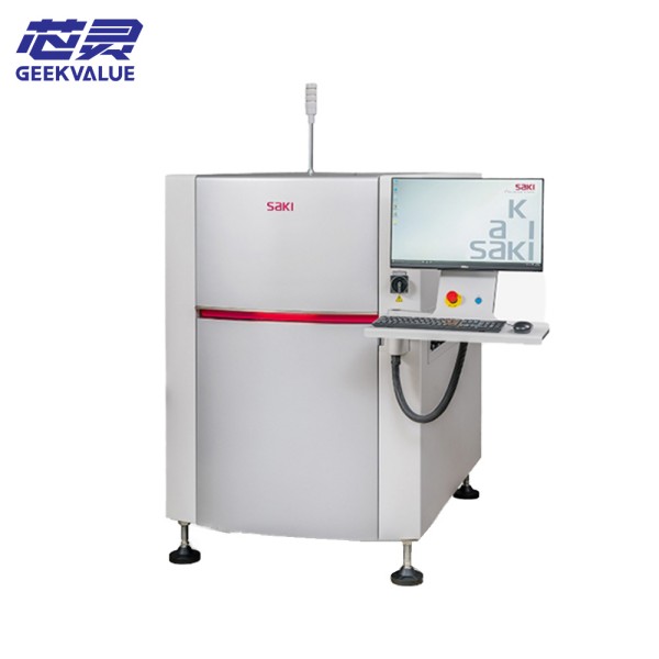
SAKI BF-3AXiM110 is a high-end 3D X-ray automatic inspection system (AXI), designed for high-density electronic assembly (such as BGA, CSP, PoP) and complex packaged devices (such as SiP, Flip Chip). It uses micro-focus X-ray imaging + CT scanning technology to achieve non-destructive testing of the internal structure of PCBs, solve hidden solder joints, internal voids, welding cracks and other defects that traditional AOI/SPI cannot reach, and is widely used in high-end manufacturing fields such as automotive electronics, aerospace, and medical equipment.
2. Core competitive advantages
✅ Ultra-high resolution 3D imaging
Nano-focus X-ray tube: minimum focus size ≤1μm, can clearly identify 0.1mm micropores and 01005 component solder joints.
CT tomography (optional): supports multi-angle 3D reconstruction, accurately locates the three-dimensional coordinates and volume of defects.
✅ Intelligent defect analysis engine
AI deep learning algorithm: automatically classifies complex defects such as voids, cold solders, and bridging, with a false alarm rate of <1%.
Multimodal detection: supports 2D/3D mode switching to adapt to different detection needs (such as fast full inspection + CT scanning of key areas).
✅ Efficient detection and automation
High-speed scanning: The maximum detection speed reaches 200mm/s (2D mode), supporting dual-lane parallel detection.
3. Core detection functions
🔹 Typical defect detection capabilities
Defect type Detection principle Application cases
Void in solder joints 3D-CT analysis of bubble distribution inside solder Automotive BGA solder joint reliability verification
Cold solder X-ray grayscale contrast to identify unmelted solder areas Detection of key solder joints in medical equipment
Bridging 3D model reconstruction of adjacent solder joint connectivity High-density CSP packaging for mobile phone motherboards
Component misalignment 2D/3D comparison of component and pad position Aerospace PCB assembly precision control
🔹 Special application scenarios
Copper pillar bump detection: measure the height consistency of micro bumps (applicable to Flip Chip).
Through hole filling rate analysis: quantify the metallization integrity of PCB copper-plated holes (PTH).
Failure analysis (FA): locate hidden faults such as short circuits and cracks in the inner layer of PCB.
4. Hardware configuration and specifications
📌 Key hardware components
X-ray generator:
Voltage range: 30kV-110kV (adjustable), power ≥90W.
Focus size: 1μm (minimum), life ≥20,000 hours.
Detector:
Flat-panel detector resolution: 2048×2048 pixels, dynamic range 16bit.
Mechanical system:
Sample stage load: ≤5kg, travel 500mm×500mm×200mm (XYZ).
Tilt mechanism: ±60° (optional 360° rotation CT mode).
📌 Technical Parameters Summary Table
Parameters BF-3AXiM110 Specifications
X-ray resolution ≤1μm (2D mode), 5μm (3D-CT)
Maximum PCB size 510mm × 460mm
Detection speed ≤200mm/s (2D), ≤30min/board (full CT scan)
Void detection sensitivity ≥5μm (diameter)
Radiation safety Leakage dose <1μSv/h, in line with GBZ 117-2022
Communication interface SECS/GEM, TCP/IP, OPC UA
5. Industry application cases
🚗 Automotive electronics
ECU control module: Detect BGA solder joint void rate (required <15%) to ensure reliability in high temperature and high vibration environments.
Automotive radar PCB: Verify the quality of through-hole filling of high-frequency signal paths.
🛰️ Aerospace
Satellite communication module: CT scans the inner layer interconnection of multi-layer boards to eliminate the risk of micro short circuits.
Flight control system: Detect the integrity of leadless solder joints of high-pin-count QFN packages.
🏥 Medical devices
Implantable electronics: Ensure that solder joints are free of toxic metal contaminants (such as lead residues).
Imaging equipment PCB: Verify the insulation spacing of high-voltage circuits.
6. Differentiation from competitors
Dimension SAKI BF-3AXiM110 Conventional X-Ray equipment
Resolution ≤1μm (micro focus) Usually 3~5μm (closed tube)
Detection mode 2D+3D-CT integration Most only support 2D or simple tomography
Intelligence AI automatic defect classification + SPC trend analysis Rely on manual interpretation
Extensibility Optional energy spectrum analysis (EDS) module Fixed function
8. Summary and recommendation
SAKI BF-3AXiM110 has become a quality guardian of high-reliability electronic manufacturing through nano-scale X-ray imaging, intelligent 3D reconstruction and Industry 4.0 integration capabilities. Its core value lies in:
Defect prevention: intercept potential faults at an early stage and reduce after-sales repair costs.
Process optimization: feedback to welding parameter adjustment through quantitative data (such as void rate).
Compliance guarantee: meet strict standards such as automotive regulations, medical, and aerospace.