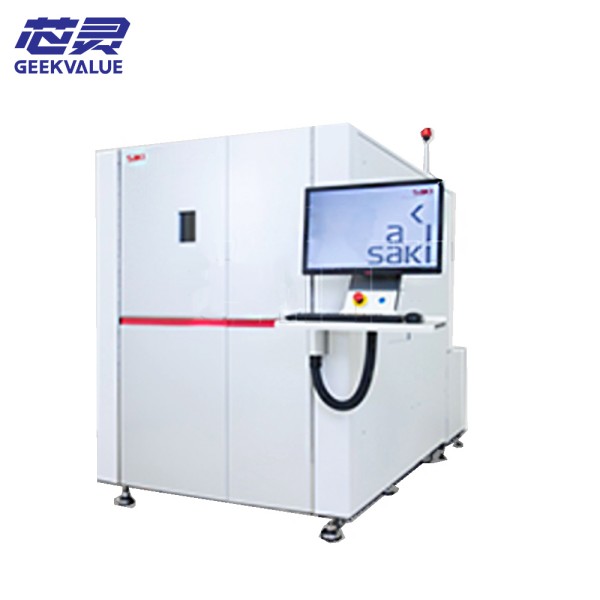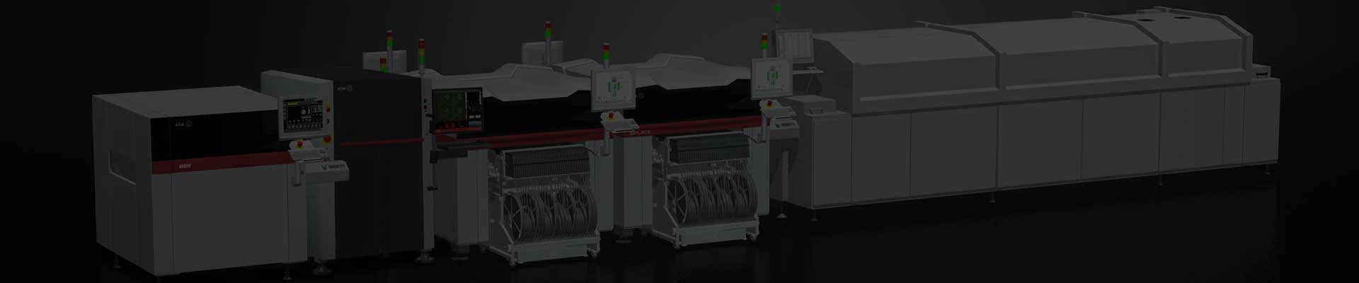
SAKI BF-3AXiM200 is a high-end 3D X-ray automatic inspection system (AXI), designed for high-density electronic packaging (such as BGA, CSP, Flip Chip) and complex PCB assembly. It uses micro-focus X-ray imaging + CT scanning technology to achieve non-destructive inspection of hidden solder joints and internal defects, and is widely used in automotive electronics, aerospace, 5G communications, medical equipment and other fields with extremely high reliability requirements.
2. Core specifications and technical parameters
📌 Hardware configuration
Item Parameters
X-ray source Open microfocus tube, voltage range 30kV-160kV
Focus size 0.5μm (minimum), resolution submicron level
Detector High-sensitivity flat-panel detector, resolution 2048×2048
Maximum detection PCB size 510mm × 460mm (larger size can be customized)
CT scanning capability Support 360° tomography, layer accuracy 3μm
Motion system High-precision linear module, repeatable positioning accuracy ±2μm
Radiation safety Leakage dose <1μSv/h, in line with international safety standards
📌 Performance indicators
Detection speed:
2D mode: ≤250mm/s (high-speed scanning)
3D-CT mode: 10-30 minutes/board (depending on resolution requirements)
Defect detection sensitivity:
Can identify solder joint voids ≥3μm
Support Solder joint quality analysis of 01005 components (0.4mm×0.2mm)
3. Core functions and roles
🔹 1. High-precision defect detection
Welding defects:
Cold Solder, Bridging, Void, Solder Ball
Assembly problems:
Component misalignment, pin crack, foreign material
🔹 2. 3D-CT tomography (optional)
Three-dimensional reconstruction: Generate a three-dimensional model of solder joints/through holes through multi-angle projection, and quantitatively analyze:
Void rate (Void%), solder filling height, coplanarity
Internal structure analysis:
PCB inner layer short circuit, copper plated hole (PTH) metallization integrity
🔹 3. Intelligent analysis and data management
AI automatic classification: Deep learning algorithm automatically marks defect types (such as IPC-A-610 Class 3 standard).
SPC process control: real-time statistics of solder joint parameters (volume, height), and generation of trend reports.
MES integration: support SECS/GEM protocol, and interoperate with factory management system data.
4. Product advantages
✅ Ultra-high resolution imaging
0.5μm micro-focus X-ray: clearly capture the solder joint details of ultra-fine pitch BGA (0.3mm pitch).
16-bit grayscale detector: distinguish small density differences (such as the contrast between solder paste and copper layer).
✅ Efficient multi-mode detection
2D fast scanning: suitable for full inspection of production line, with a speed of 250mm/s.
3D-CT in-depth analysis: high-precision tomography for key areas (such as automotive ECU).
✅ Intelligence and automation
One-button operation: preset inspection program, support offline programming (OLP).
Automatic calibration: reduce manual intervention and improve equipment stability.
✅ Safety and compliance
Radiation protection: lead glass shielding + interlocking device to ensure safe operation.
Industry certification: Meets IPC, IATF 16949 (automotive), ISO 13485 (medical) standards.
5. Typical application scenarios
🚗 Automotive electronics
ADAS radar module: Detect solder voids in high-frequency signal paths.
Battery management system (BMS): Ensure welding reliability of high-current paths.
📡 5G communications
Millimeter wave antenna PCB: Verify the welding quality of RF components (such as GaN devices).
Base station power amplifier: Analyze the thermal fatigue risk of large-size pads.
🛰️ Aerospace
Satellite control system: 3D defect detection of inner layer interconnects of multi-layer boards.
Flight control module: Non-destructive testing of high-pin count QFN packages.
🏥 Medical equipment
Implantable electronics: Detect solder joint biocompatibility (lead-free residue).
Imaging equipment PCB: Insulation spacing verification of high-voltage circuits.
6. Differentiation from competitors
Function SAKI BF-3AXiM200 Conventional X-Ray equipment
Resolution 0.5μm (industry top) Usually 1~5μm
Detection mode 2D+3D-CT integration, support tilt scanning Most only support 2D or simple tomography
Intelligent AI automatic defect classification + closed-loop process feedback Rely on manual experience to judge
Extensibility Optional energy spectrum analysis (EDS) module Fixed function
7. Summary
SAKI BF-3AXiM200 has become the ultimate detection solution for high-reliability electronic manufacturing with submicron resolution, intelligent CT scanning and Industry 4.0 integration capabilities. Its core value lies in:
Zero defect control: intercept potential failures at an early stage and reduce after-sales risks.
Data-driven optimization: improve welding processes through quantitative analysis (such as void rate).
Full industry adaptation: meet the most stringent standards such as automotive, medical, and aerospace.