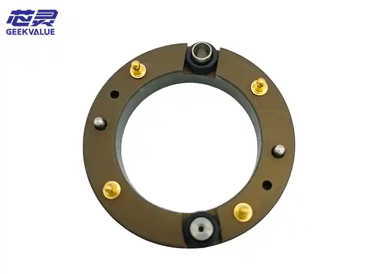
ASM 54 PCB Camera (commonly known as PCB Camera 54) is a key visual component in Siemens ASM (formerly SIPLACE) placement machines, mainly used for fiducial mark recognition and global positioning of PCBs (printed circuit boards). It ensures that placement machines can accurately identify the position, angle and deformation of PCBs, thereby achieving high-precision placement.
2. Main functions
PCB fiducial mark detection
Identify optical fiducials (fiducial) on PCBs and correct PCB position deviations (X/Y/θ).
Supports multiple fiducial point types such as circular, cross, square, etc.
PCB global positioning (Global Alignment)
Detect the overall offset and distortion (Warpage) of PCBs to ensure placement accuracy.
PCB panel recognition (Panel Recognition)
Applicable to multi-panel (Panelized PCB) production, automatically identify panel layout.
PCB Dimension Check
Optional function, used to check whether the PCB size meets the requirements.
3. Technical Specifications
Parameter Specifications
Camera Type High-resolution CCD/CMOS camera (specific model depends on the model)
Resolution Usually 5-10μm/pixel (depending on the optical magnification)
Field of View (FOV) 20mm × 20mm (typical value, adjustable)
Light Source Ring LED lighting (adjustable brightness), supports multi-angle lighting
Communication Interface GigE (Gigabit Ethernet) or Camera Link
Frame Rate (FPS) 30-60fps (depending on resolution and lighting conditions)
Applicable PCB Color Green, blue, black, white, etc. (adaptive adjustment)
Software Support SIPLACE Pro / ASM Works / SIPLACE OS
4. Structural Composition
(1) Optical System
Lens: High-precision industrial lens, supports autofocus or manual focus.
Filter: Optional polarizing filter to reduce reflection interference.
(2) Lighting system
Ring LED light source: adjustable at multiple angles to suit different PCB surfaces (matte, glossy, high reflective).
Coaxial light (optional): for highly reflective PCBs (such as metal substrates).
(3) Mechanical structure
Camera bracket: adjustable in height and angle to ensure optimal imaging.
Anti-vibration design: reduces the impact of machine vibration on imaging.
(4) Electronic system
Image acquisition card: responsible for high-speed image transmission.
Trigger signal interface: synchronized with the placement machine PLC to ensure accurate shooting timing.
5. Workflow
PCB enters the machine → conveyor belt locates the PCB.
The camera moves above the reference point → takes an image of the PCB reference point.
Image processing → calculates the X/Y offset and rotation angle (θ) of the PCB.
Data is fed back to the placement system → automatically adjusts the placement coordinates.
The placement machine starts placement → ensures that all components are accurately placed.
6. Precautions for use
(1) Installation and calibration
Camera height calibration: Make sure the focal length is correct, otherwise the recognition accuracy will decrease.
Adjust the brightness of the light source: Optimize the lighting for different PCB colors to avoid overexposure or underexposure.
Design specifications for reference points:
Recommended size: 1.0mm - 2.0mm (circular/cross-shaped).
Avoid overlapping with pads and silk screens.
(2) Daily maintenance
Clean the lens regularly: Wipe with a dust-free cloth and alcohol to prevent dust from affecting the image.
Check the LED life: Aging LEDs will cause a decrease in recognition rate and need to be replaced regularly.
Avoid mechanical collisions: Camera position offset will cause recognition errors.
(3) Software optimization
Adjust the recognition threshold: Adapt to different PCB surfaces (e.g. black PCBs require higher contrast).
Optimize the reference point search area (ROI): Narrowing the range can increase recognition speed.
7. Common faults and solutions
Fault phenomenon Possible cause Solution
Reference point recognition failed 1. Camera focus is inaccurate
2. Light source brightness is not appropriate
3. PCB reference point contamination 1. Recalibrate focus
2. Adjust LED brightness
3. Clean PCB or replace reference point
Slow recognition speed 1. Complex image processing algorithm
2. Communication delay 1. Optimize ROI (reduce search range)
2. Check network cable or replace image acquisition card
Blurred image 1. Lens contamination
2. Vibration interference 1. Clean lens
2. Check if the camera fixing screws are loose
Misidentification (misalignment) 1. PCB deformation
2. Poor reference point design 1. Add more reference points (3-4)
2. Modify PCB design
8. Upgrade and Alternative Solutions
Upgrade to a higher resolution camera (e.g. 10μm → 5μm) to improve the recognition of small fiducials.
Replace infrared (IR) camera: suitable for special PCB materials (e.g. ceramic substrates).
Add AI recognition algorithm: for high-precision positioning of complex PCBs (e.g. flexible boards FPC).
9. Summary
ASM 54 PCB camera is the core visual component of the SMT placement machine and directly affects the placement accuracy. Its high-resolution imaging, adjustable light source and intelligent recognition algorithm enable it to adapt to various PCB types. Regular calibration, cleaning and parameter optimization are the key to ensure its stable operation.