Toliau pateikiamas išsamus SAKI 3D AOI 3Di MS2 įvadas, kuriame aptariamas jo padėties nustatymas, pagrindinė technologija, funkcinės savybės, pritaikymas pramonėje ir konkurenciniai pranašumai. Turinys sudarytas remiantis bendraisiais pramonės standartais ir panašios įrangos tipinėmis charakteristikomis. Dėl konkrečių parametrų žr. oficialią informaciją:
1. Įrangos apžvalga
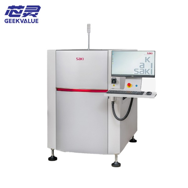
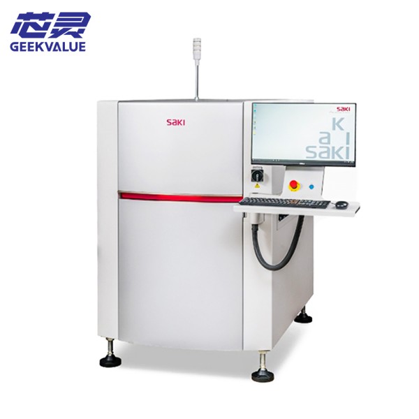
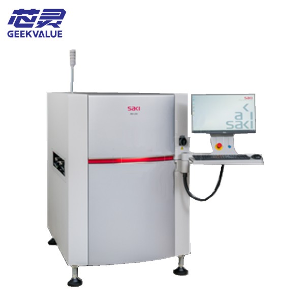
Modelis: SAKI 3Di MS2
Tipas: 3D automatinė optinė tikrinimo įranga (AOI)
Pagrindinė paskirtis: Naudojama didelio tikslumo trimačiam kokybės patikrinimui po PCB surinkimo SMT (paviršinio montavimo technologijos) gamybos linijose, siekiant užtikrinti, kad litavimo jungtys, komponentų tvirtinimas ir kt. atitiktų proceso standartus.
Techninis maršrutas: sujungti kelių kampų 3D vaizdavimą su dirbtinio intelekto algoritmais, siekiant išspręsti tradicinio 2D AOI apribojimus aukščio aptikimo ir sudėtingų komponentų srityje.
2. Pagrindinės technologijos ir aparatinės įrangos konfigūracija
(1) 3D vaizdavimo sistema
Techninis principas:
Lazerinė trianguliacija arba struktūrizuota šviesos projekcija, naudojant daugiaašį skenavimą, siekiant gauti trimačius duomenis, tokius kaip litavimo jungties aukštis, tūris, forma ir kt.
Skiriamoji geba gali siekti mikronų lygį (pvz., 1 μm Z ašies pakartojamumą), todėl galima aptikti labai mažus komponentus (pvz., 01005 korpusą).
Šviesos šaltinio sistema:
Daugiaspektris kombinuotas šviesos šaltinis (pvz., RGB + infraraudonieji spinduliai) pagerina defektų (pvz., tiltelių, šaltojo litavimo jungčių) kontrastą, apšviesdamas skirtingais kampais.
(2) Didelio tikslumo judesio valdymas
Didelės spartos linijinis variklis: užtikrina greitą padėties nustatymą ir nuskaitymą, prisitaiko prie didelio našumo gamybos linijų (pvz., UPH ≥ 300 plokščių per valandą).
Dviejų takelių parinktis: kai kurios konfigūracijos palaiko dviejų takelių sinchroninį aptikimą, siekiant pagerinti pralaidumą.
(3) Pažangi programinės įrangos platforma
DI defektų klasifikacija:
Remiantis gilaus mokymosi algoritmų biblioteka, jis automatiškai identifikuoja prastas litavimo jungtis (nepakankamas litavimas, tuštumos, poslinkiai ir kt.) ir komponentų defektus (ženkliukus, netinkamas dalis ir kt.), sumažindamas klaidingų aliarmų skaičių.
Formulės valdymas:
Palaiko programavimą ir modeliavimą neprisijungus, greitai perjungia gaminių modelius ir sutrumpina linijų keitimo laiką.
3. Pagrindinės funkcijos ir aptikimo galimybės
(1) Litavimo jungčių aptikimas
3D parametrų kiekybinis įvertinimas: išmatuokite litavimo jungties aukštį, tūrį, kontaktinį kampą ir kt., ir tiksliai įvertinkite defektus, tokius kaip šalti litavimo jungtys, tilteliai ir litavimo rutuliukai.
BGA/CSP patikra: nuskaitykite paslėptus litavimo sujungimus per komponento kraštą, kad išspręstumėte 2D AOI aklosios zonos problemą.
(2) Komponentų išdėstymo patikrinimas
Buvimas / poliškumas: nustatykite trūkstamus, apverstus ir neteisingus komponentus.
Padėties tikslumas: aptikti poslinkį ir pakreipimą (pvz., QFN šoninės litavimo kojelės).
(3) Suderinamumas
Plokštės tipo pritaikymas: lanksti plokštė (FPC), standi plokštė, stora varinė plokštė ir kt.
Komponentų asortimentas: nuo 0201 mikro komponentų iki didelių jungčių ir ekranuojančių dangtelių.
4. Pramonės taikymo scenarijai
Didelio patikimumo laukas:
Automobilių elektronika: ECU, jutiklių modulis (atitinka IPC-A-610 3 klasės standartą).
Medicinos įranga: implantuojama prietaiso PCB plokštė, nereikalaujanti jokių defektų.
Didelio tankio pakuotė:
Išmaniojo telefono pagrindinė plokštė (POP pakuotė), 5G ryšio modulis.
Automatizuotos gamybos linijos integravimas:
Susiejimas su SPI (litavimo pastos aptikimo), refly krosnies ir kitos įrangos duomenimis, siekiant visapusiškos proceso kokybės kontrolės.
5. Konkurencinio pranašumo analizė
(1) Palyginti su tradiciniu 2D AOI
Mažiau klaidingų vertinimų: 3D aukščio duomenys vengia spalvų ir atspindžių interferencijos.
Platesnis aprėpties plotas: gali aptikti paslėptus litavimo sujungimus (pvz., apatinius gnybtų komponentus).
(2) Palyginti su panašiu 3D AOI
Greičio ir tikslumo pusiausvyra: SAKI lygiagretaus skenavimo technologija atsižvelgia tiek į aptikimo greitį, tiek į detalių skiriamąją gebą.
Atvira duomenų sąsaja: palaiko integraciją su MES/SPC sistemomis, kad padėtų kurti išmaniąsias gamyklas.
(3) Sąnaudų efektyvumas
Sumažinkite pakartotinio patikrinimo išlaidas: didelis tikslumas sumažina rankinio pakartotinio patikrinimo valandas.
Profilaktinė priežiūra: iš anksto aptikkite proceso svyravimus (pvz., nenormalų litavimo pastos spausdinimą) atlikdami tendencijų analizę.
6. Papildomos papildomos funkcijos
Dvipusis patikrinimas: visiškas dvipusis PCB patikrinimas vienu užspaudimu.
Dirbtinio intelekto savioptimizavimas: nuolat mokosi naujų defektų modelių ir dinamiškai atnaujina tikrinimo standartus.
Nuotolinė diagnostika: įrangos stebėjimas ir priežiūra realiuoju laiku per daiktų internetą (IoT).
7. Tipiniai vartotojų problemų sprendimai
Problema: Atšaukimo rizika dėl praleistos automobilių spausdintinių plokščių litavimo jungčių patikros.
→ 3Di MS2 sprendimas: Atlikus 3D litavimo jungčių tūrio analizę, 100 % litavimo jungčių, kurių aukštis nepakankamas, yra perimamos.
Problema: Dažni gamybos linijų pakeitimai lemia daug laiko reikalaujantį AOI derinimą.
→ Sprendimas: neprisijungus pasiekiama formulių biblioteka + dirbtinio intelekto pritaikymas, sutrumpinantis perjungimo laiką iki 10 minučių.