The following is a comprehensive introduction to SAKI 3D AOI 3Di MS2, covering its positioning, core technology, functional features, industry applications and competitive advantages. The content is organized based on industry general standards and typical characteristics of similar equipment. For specific parameters, please refer to official information:
1. Equipment Overview
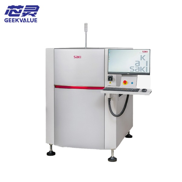
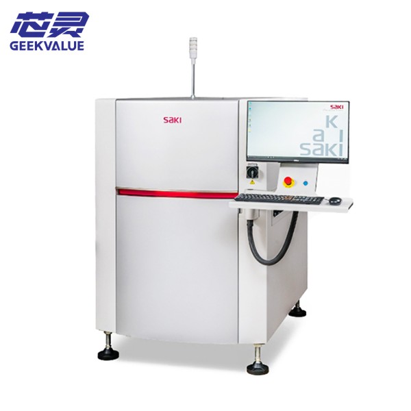
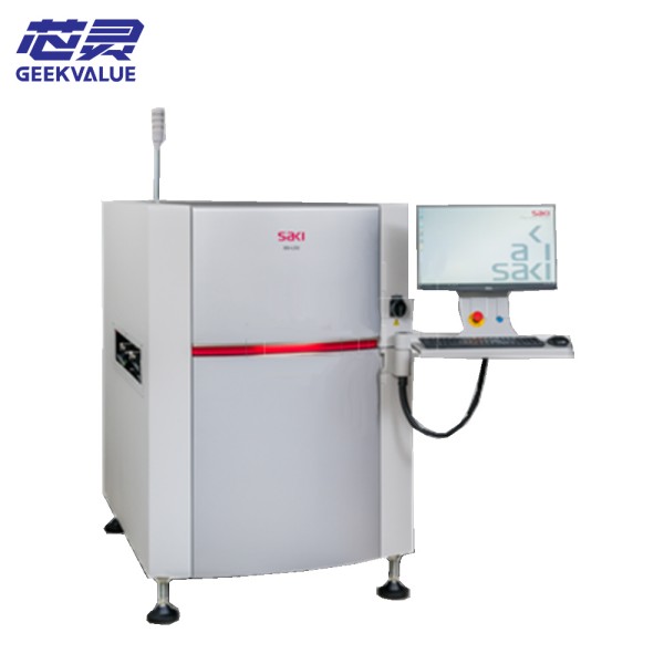
Model: SAKI 3Di MS2
Type: 3D automatic optical inspection equipment (AOI)
Core purpose: Used for high-precision three-dimensional quality inspection after PCB assembly in SMT (surface mount technology) production lines to ensure that solder joints, component mounting, etc. meet process standards.
Technical route: Combine multi-angle 3D imaging with AI algorithms to solve the limitations of traditional 2D AOI in height detection and complex components.
2. Core technology and hardware configuration
(1) 3D imaging system
Technical principle:
Laser triangulation or structured light projection, through multi-axis scanning to obtain three-dimensional data such as solder joint height, volume, shape, etc.
The resolution can reach micron level (such as 1μm Z-axis repeatability), supporting the detection of tiny components (such as 01005 package).
Light source system:
Multi-spectral combined light source (such as RGB+infrared) enhances defect contrast (such as bridging, cold solder joints) by lighting at different angles.
(2) High-precision motion control
High-speed linear motor: Achieve fast positioning and scanning, adapt to high-beat production lines (such as UPH ≥ 300 boards/hour).
Dual track option: Some configurations support dual-track synchronous detection to improve throughput.
(3) Intelligent software platform
AI defect classification:
Based on the deep learning algorithm library, it automatically identifies poor solder joints (insufficient solder, voids, offsets, etc.) and component defects (tombstones, wrong parts, etc.), reducing the false alarm rate.
Formula management:
Supports offline programming and simulation, quickly switches product models, and reduces line change time.
3. Core functions and detection capabilities
(1) Solder joint detection
3D parameter quantification: Measure solder joint height, volume, contact angle, etc., and accurately judge defects such as cold solder joints, bridging, and solder balls.
BGA/CSP inspection: Scan hidden solder joints through the edge of the component to solve the blind spot problem of 2D AOI.
(2) Component placement inspection
Existence/polarity: Identify missing, reversed, and wrong components.
Position accuracy: Detect offset and tilt (such as QFN side solder feet).
(3) Compatibility
Board type adaptation: flexible board (FPC), rigid board, thick copper board, etc.
Component range: 0201 micro components to large connectors and shielding covers.
4. Industry application scenarios
High reliability field:
Automotive electronics: ECU, sensor module (compliant with IPC-A-610 Class 3 standard).
Medical equipment: Implantable device PCB, requiring zero defects.
High-density packaging:
Smartphone motherboard (POP packaging), 5G communication module.
Automated production line integration:
Link with SPI (solder paste detection), reflow oven and other equipment data to achieve full process quality control.
5. Competitive Advantage Analysis
(1) Compared with traditional 2D AOI
Fewer misjudgments: 3D height data avoids color and reflection interference.
Wider coverage: Can detect hidden solder joints (such as bottom terminal components).
(2) Compared with similar 3D AOI
Balance between speed and accuracy: SAKI's parallel scanning technology takes into account both detection speed and detail resolution.
Open data interface: Supports integration with MES/SPC systems to help build smart factories.
(3) Cost-effectiveness
Reduce re-inspection costs: High accuracy reduces manual re-inspection hours.
Preventive maintenance: Detect process fluctuations (such as abnormal solder paste printing) in advance through trend analysis.
6. Optional extended functions
Double-sided inspection: Complete double-sided PCB inspection in one clamping.
AI self-optimization: Continuously learn new defect patterns and dynamically update inspection standards.
Remote diagnosis: Real-time equipment monitoring and maintenance through the Internet of Things (IoT).
7. Typical user pain point solutions
Problem: Risk of recall due to missed inspection of automotive PCB solder joints.
→ 3Di MS2 solution: Through 3D solder joint volume analysis, 100% of solder joints with insufficient height are intercepted.
Problem: Frequent production line changes lead to time-consuming AOI debugging.
→ Solution: Offline formula library + AI adaptation, shortening the changeover time to within 10 minutes.