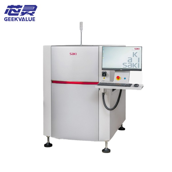
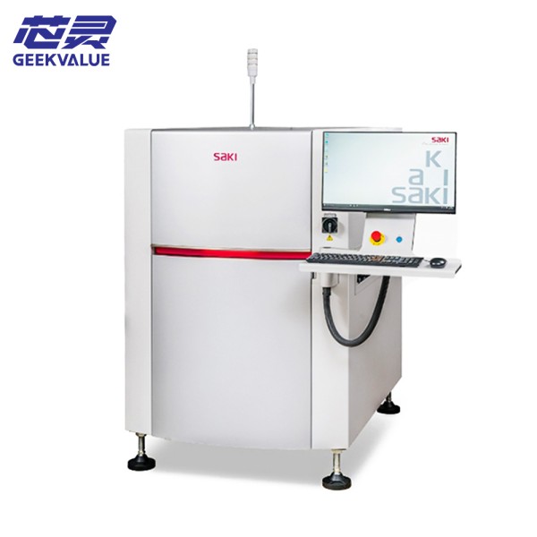
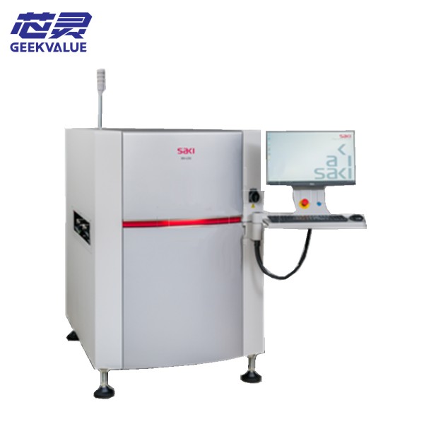
The following is a comprehensive and detailed introduction to SAKI 2D AOI BF-TristarⅡ
1.1 Optical Imaging Principle
Bright Field Illumination Technology:
The PCB surface is illuminated by a multi-angle high-brightness LED light source (red/green/blue/white combination), and the reflectivity difference between the solder joint and the background material is used to capture high-contrast images. Smooth solder joints show mirror reflection (bright area), while defective areas (such as cracks and insufficient tin) are displayed as dark areas due to diffuse reflection.
Dual-track synchronous imaging:
Two sets of high-resolution linear array cameras (up to 10μm/pixel) scan the upper and lower surfaces of the PCB synchronously, combined with a high-speed image processor for real-time analysis.
1.2 Defect Detection Logic
Template matching: Compare the position and shape differences between the standard solder joint/component library and the actual image.
Grayscale/geometric analysis: Determine defects such as cold solder joints and bridging by solder joint brightness distribution and contour integrity.
AI-assisted classification: Deep learning algorithms extract features for complex defects (such as BGA solder ball collapse) to reduce misjudgment.
2. Core advantages
Advantage dimensions Specific performance
Detection accuracy Can identify 01005 components (0.4mm×0.2mm) and micron-level solder joint defects (such as 5μm cracks).
Speed and efficiency The dual-track detection design achieves 0.25 seconds/point, which is more than 30% faster than the single-track AOI.
Adaptability Supports complex scenarios such as rigid PCB, FPC (flexible board), and highly reflective lead-free solder.
Intelligent AI algorithm self-learning optimization, false alarm rate <0.1%, reducing manual re-inspection costs.
Extensibility Can be linked with SPI, ICT and other equipment to build a full-process quality closed loop.
3. Technical features
3.1 Hardware design
Multi-spectral lighting system:
8-directional programmable LED light source, support dynamic adjustment of wavelength and angle, to meet the detection needs of different solders (such as SAC305 and SnPb).
High-rigidity mechanical structure:
Marble base + linear motor drive to ensure scanning stability (repeat positioning accuracy ±5μm).
3.2 Software Functions
3D simulation analysis:
Reconstruct solder joint height information based on 2D images, and indirectly detect 3D defects such as warpage and insufficient solder paste.
Recipe management:
Can store 1000+ inspection programs, and support one-click switching of product models.
4. Specifications
Category Detailed specifications
Inspection range PCB size: 50mm×50mm ~ 510mm×460mm (customizable extra-large board)
Optical resolution Standard 10μm/pixel (up to 5μm/pixel optional)
Inspection speed 0.25~0.5 seconds/inspection point (depending on complexity)
Communication interface SECS/GEM, TCP/IP, RS-232, support MES system integration
Power requirements AC 200-240V, 50/60Hz, power consumption ≤1.5kW
5. Functional modules
5.1 Core inspection functions
Solder joint inspection:
SMT solder joints: BGA solder ball missing, bridging, cold soldering, offset.
Through-hole solder joints: poor tin penetration, holes.
Component inspection:
Polarity reversal, wrong parts, tombstone, rollover, damage.
Appearance inspection:
Board surface pollution, blurred characters, scratches on solder mask.
5.2 Auxiliary functions
SPI data linkage: import solder paste inspection results, correlate and analyze solder joint molding quality.
NG marking: trigger the marking machine or labeling machine to mark the defect position.
Data traceability: store inspection images and results, support batch quality statistical analysis.
6. Actual role
6.1 Quality control
Defect interception rate>99%: replace manual visual inspection at the end of the SMT production line to eliminate missed inspections.
Process optimization: feedback to the calibration parameters of the placement machine through defect distribution statistics (such as concentrated offset).
6.2 Cost control
Reduce rework costs: early detection of defects can reduce scrap losses in subsequent processes.
Improve pass rate: reduce unnecessary downtime caused by misjudgment through high-precision inspection.
6.3 Industry Applications
Consumer electronics: detection of micro solder joints on mobile phone motherboards.
Automotive electronics: reliability assurance of ECU boards in high temperature and high vibration environments.
Medical equipment: meets the strict quality inspection requirements of ISO 13485.
7. Summary
SAKI BF-TristarⅡ takes "high precision + high efficiency + intelligence" as its core, and through the innovative combination of multi-spectral optical system, AI algorithm, and dual-track architecture, it has become a cost-effective solution in the field of 2D AOI, especially suitable for precision electronics manufacturing that pursues zero defects.